Certus Optic NanoScanTechnology Applications: reasoned innovations
advertisement
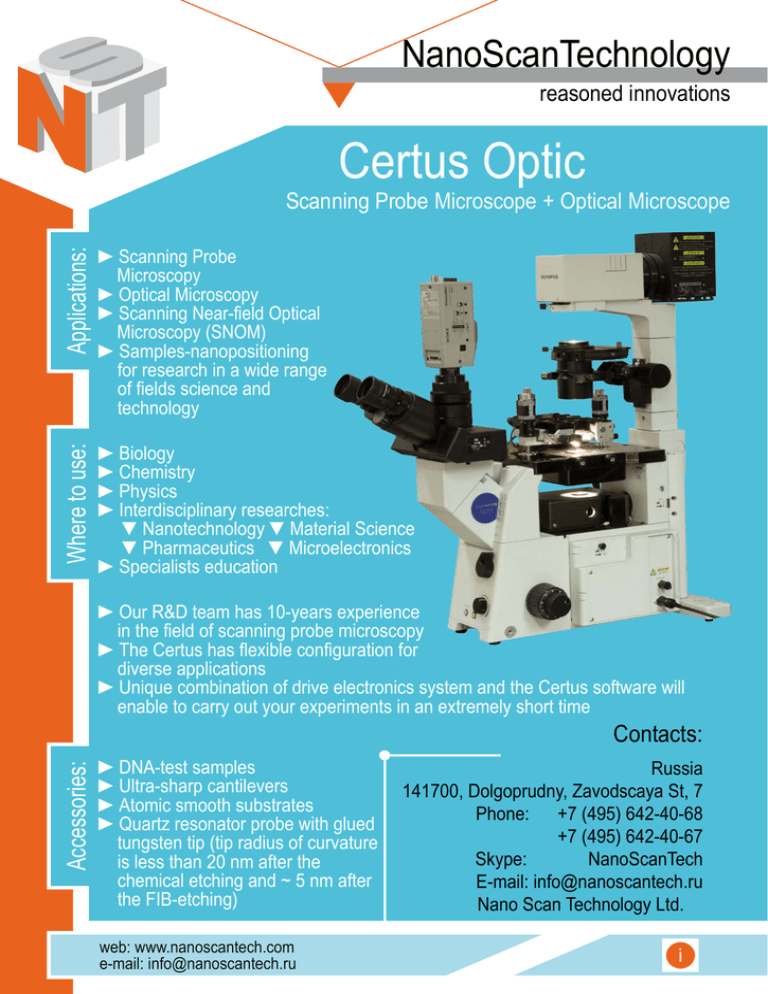
NanoScanTechnology reasoned innovations Certus Optic Applications: ►Scanning Probe Microscopy ►Optical Microscopy ►Scanning Near-field Optical Microscopy (SNOM) ►Samples-nanopositioning for research in a wide range of fields science and technology Where to use: Scanning Probe Microscope + Optical Microscope ►Biology ►Chemistry ►Physics ►Interdisciplinary researches: ▼Nanotechnology ▼Material Science ▼Pharmaceutics ▼Microelectronics ►Specialists education ►Our R&D team has 10-years experience in the field of scanning probe microscopy ►The Certus has flexible configuration for diverse applications ►Unique combination of drive electronics system and the Certus software will enable to carry out your experiments in an extremely short time Accessories: Contacts: ►DNA-test samples ►Ultra-sharp cantilevers ►Atomic smooth substrates ►Quartz resonator probe with glued tungsten tip (tip radius of curvature is less than 20 nm after the chemical etching and ~ 5 nm after the FIB-etching) web: www.nanoscantech.com e-mail: info@nanoscantech.ru Russia 141700, Dolgoprudny, Zavodscaya St, 7 Phone: +7 (495) 642-40-68 +7 (495) 642-40-67 Skype: NanoScanTech E-mail: info@nanoscantech.ru Nano Scan Technology Ltd. i XY Stage: Microscope Controller: Scanning head: SPM-scanning head ►XY range 100x100 μm ►Residual nonlinearity 0.003 %. ►Angle tilting < 0.01 ° over the full range ►Minimum scan step 0.1 nm ►Plan deviation < 1 nm ►Temperature drift < 1 nm/h ►Resonant frequency XY — 1 kHz ►Maximum sample size 50x50x30 mm ►Мaximum sample weight — 100 g ►Maximum scanning speed 10 Hz (line/sec) ►Drive digital controller combined USB 2.0 interface ►Up to 6 channels of piezoelectric scanners with “closed-loop” system control ►Possibility of carrying out long-continued studies using external detectors Software: The Certus Optic features: ►XYZ – plane scanner with “closed-loop” system based on three capacitance sensors without second order scanning plane distortion ►Optical convenient design of SPM-head allows to keep out standard microscopic functions, easy viewing of scanning workspace and mounting of additional objective ►Plane vertical landing of SPM-probe ►Quick-detachable SPM-probe coupling unit for one-touch changing of SPM procedures: AFM to NSOM for example XY – sample scanning stage ►Modern cross-platform simultaneous driven software for all the Certus Optic units ►Built-in capabilities of the collected data basic processing and exporting into specialized software ◄The periodic structure Si/SiO2 image obtained with AFM contact mode. Dimension scan 100x100 μm, 1024x1024 points. High linearity is clearly observed to prove positioning system performance. The image DNA moleculeson mica, data obtained in tapping mode. Dimension scan 1x1 μm,512x512 points.► web: www.nanoscantech.com e-mail: info@nanoscantech.ru i
