10-Bit, A/D Converter AD571 1.0
advertisement
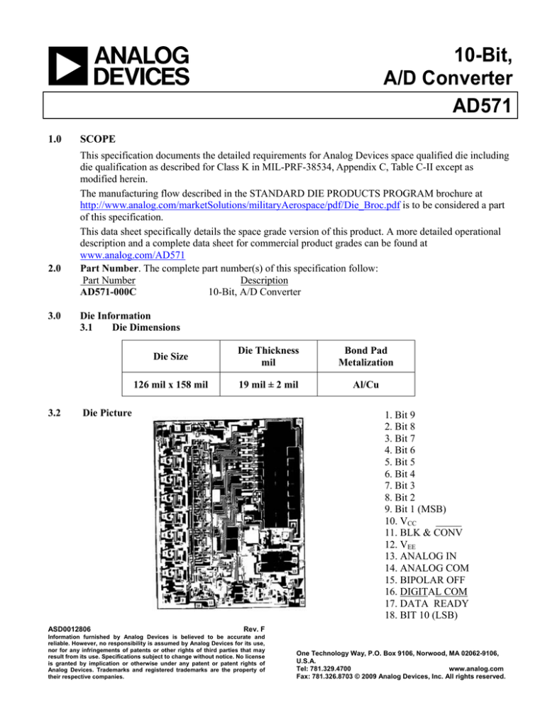
10-Bit, A/D Converter AD571 1.0 2.0 3.0 3.2 SCOPE This specification documents the detailed requirements for Analog Devices space qualified die including die qualification as described for Class K in MIL-PRF-38534, Appendix C, Table C-II except as modified herein. The manufacturing flow described in the STANDARD DIE PRODUCTS PROGRAM brochure at http://www.analog.com/marketSolutions/militaryAerospace/pdf/Die_Broc.pdf is to be considered a part of this specification. This data sheet specifically details the space grade version of this product. A more detailed operational description and a complete data sheet for commercial product grades can be found at www.analog.com/AD571 Part Number. The complete part number(s) of this specification follow: Part Number Description AD571-000C 10-Bit, A/D Converter Die Information 3.1 Die Dimensions Die Size Die Thickness mil Bond Pad Metalization 126 mil x 158 mil 19 mil ± 2 mil Al/Cu Die Picture ASD0012806 1. Bit 9 2. Bit 8 3. Bit 7 4. Bit 6 5. Bit 5 6. Bit 4 7. Bit 3 8. Bit 2 9. Bit 1 (MSB) 10. VCC _____ 11. BLK & CONV 12. VEE 13. ANALOG IN 14. ANALOG COM 15. BIPOLAR OFF 16. DIGITAL COM 17. DATA READY 18. BIT 10 (LSB) Rev. F Information furnished by Analog Devices is believed to be accurate and reliable. However, no responsibility is assumed by Analog Devices for its use, nor for any infringements of patents or other rights of third parties that may result from its use. Specifications subject to change without notice. No license is granted by implication or otherwise under any patent or patent rights of Analog Devices. Trademarks and registered trademarks are the property of their respective companies. One Technology Way, P.O. Box 9106, Norwood, MA 02062-9106, U.S.A. Tel: 781.329.4700 www.analog.com Fax: 781.326.8703 © 2009 Analog Devices, Inc. All rights reserved. AD571 3.3 Absolute Maximum Ratings 1/ Negative Supply Voltage (VEE) to Digital Common....................-16.5V dc Positive Supply Voltage (VCC) to Digital Common......................+7V dc Analog Input Voltage to Analog Common...................................±15V dc Digital Input Voltage to Digital Common.....................................0V dc to VCC Digital Output Voltage to Digital Common..................................0V dc to VCC Analog Return to Digital Common...............................................±1V dc Storage Temperature Range..........................................................-65°C to +150°C Junction Temperature (TJ).............................................................+175°C Ambient Operating Temperature Range.......................................-55°C to +125°C Absolute Maximum Ratings Notes: 1/ Stresses above the absolute maximum rating may cause permanent damage to the device. Extended operation at the maximum levels may degrade performance and affect reliability. 4.0 Die Qualification In accordance with class-K version of MIL-PRF-38534, Appendix C, Table C-II, except as modified herein. (a) Qual Sample Size and Qual Acceptance Criteria – 25/2 (b) Qual Sample Package – DIP (c) Pre-screen electrical test over temperature performed post-assembly prior to die qualification. Table I - Dice Electrical Characteristics Conditions 1/ Limit Min Limit Max Units ±0.195 % FS Parameter Symbol Relative Accuracy RA Digital Input High Voltage VIH Unipolar and Bipolar major transitions ±3 codes BLK and CONV Digital Input Low Voltage VIL BLK and CONV 0.8 V Digital Input High Current IIH BLK and CONV , VIH = 5V ±100 µA Digital Input Low Current IIL ±100 µA Digital Output Low Voltage VOL 0.4 V Digital Output High Voltage VOH Full Scale Error 2/ AE Offset Error VOS Bipolar Zero Error BPZE BLK and CONV , VIL = 0V DATA READY , Bit 1 - 10, IOL = +3.2mA Bit 1 - 10, IOH = -0.5mA Unipolar Bipolar First transition Low side MSB, Transition Bipolar ASD0012806 Rev. F | Page 2 of 6 2 V 2.4 V ±40 ±20 ±0.4 % FS ±0.4 % FS mV AD571 Table I - Dice Electrical Characteristics (Continued) Parameter Three-State Leakage Current Power Supply Current Conditions Limit Limit 1/ Min Max Units Symbol IOLT ICC VOH = 5V, VOL = 0V, DNL µA 10 BLK and CONV mA -15 IEE Differential Nonlinearity 3/ ±40 Bit 1 - 10 All codes test Unipolar and Bipolar 10 Bits -16.0V ≤ VEE ≤ -13.5V Power Supply Rejection PSRR VCC = +5V +4.5V ≤ VCC ≤ +5.5V ±78.1 mV VEE = -15V Table I Notes: 1/ VCC = +5V, VEE = -15V, VIH = +2.0V, VIL = +0.8V, analog input through 15Ω to pin 13, Unipolar configuration. Also, in the Unipolar configuration pin 15 (Bipolar Offset Control) is grounded. TA = 25°C, unless otherwise specified. 2/ Full Scale Error guaranteed trimmable with 50Ω potentiometer. 3/ Minimum resolution for which no missing codes are guaranteed. ASD0012806 Rev. F | Page 3 of 6 AD571 Table II - Electrical Characteristics for Qual Samples Parameter Symbol Conditions 1/ Subgroups Limit Min Unipolar and Bipolar 1, 2, 3 major transitions ±3 codes Limit Max Units ±0.195 % of FS Relative Accuracy RA Digital Input High Voltage VIH BLK and CONV 1, 2, 3 Digital Input Low Voltage VIL BLK and CONV 1, 2, 3 0.8 V Digital Input High Current IIH 1, 2, 3 ±100 µA Digital Input Low Current IIL 1, 2, 3 ±100 µA Digital Output Low Voltage VOL 1, 2, 3 0.4 V Digital Output High Voltage VOH Full Scale Error 2/ AE BLK and CONV , VIH = 5V BLK and CONV , VIL = 0V DATA READY , Bit 1 - 10, IOL = +3.2mA Bit 1 - 10, IOH = -0.5mA Unipolar Bipolar Full Scale Temperature Drift TCAE Offset Error VOS Offset Temperature Drift TCVOS Bipolar Zero Error BPZE Bipolar Zero Temperature TCBPZE Three-State Leakage Current IOLT Power Supply Current ICC IEE Differential Nonlinearity 3/ DNL Power Supply Rejection PSRR Input Resistance Conversion Time RIN TC 1, 2, 3 All codes test Unipolar and Bipolar -16.0V ≤ VEE ≤ -13.5V VCC = +5V +4.5V ≤ VCC ≤ +5.5V VEE = -15V V 2.4 V 2, 3 1 2, 3 ±40 ±20 ±0.488 ±0.4 ±0.195 % FS % FS % FS 1 ±0.4 % FS 2, 3 ±0.195 % FS 1, 2, 3 ±40 µA 1 1 10 -15 1 10 1 First transition Low side MSB, Transition Bipolar Bipolar VOH = 5V, VOL = 0V, Bit 1 - 10 BLK and CONV 2 1, 2, 3 4 9 3 15 mV mA Bits ±78.1 mV 7 40 kΩ µs Table II Notes: VCC = +5V, VEE = -15V, VIH = +2.0V, VIL = +0.8V, analog input through 15Ω to pin 13, Unipolar 1/ configuration. Also, in the Unipolar configuration pin 15 (Bipolar Offset Control) is grounded. Full Scale Error guaranteed trimmable with 50Ω potentiometer. 2/ Minimum resolution for which no missing codes are guaranteed. 3/ ASD0012806 Rev. F | Page 4 of 6 AD571 Table III - Life Test Endpoint and Delta Parameter (Product is tested in accordance with Table II with the following exceptions) Parameter Symbol Subgroups Power Supply Current Digital Output Low Voltage Digital Output High Voltage Offset Error Bipolar Zero Error Unipolar Full Scale Error ICC VOL VOH VOS BPZE AE UNI 1 1, 2, 3 1, 2, 3 1 1 1 Bipolar Full Scale Error AE BIP 1 5.0 Post Burn In Limit Min Max Post Life Test Limit Min 10 0.4 Max Life Test Delta ±0.6 ±0.6 ±40 ±0.8 ±0.8 ±80 mA V V % FS % FS mV ±20 ±60 mV 2.4 0.4 2.4 Life Test/Burn-In Information 5.1 HTRB is not applicable for this drawing. 5.2 Burn-in is per MIL-STD-883 Method 1015 test condition B or C. 5.3 Steady state life test is per MIL-STD-883 Method 1005. ASD0012806 Rev. F | Page 5 of 6 ±1 ±0.1 ±0.24 Units AD571 Rev A B C D E F Description of Change Initiate Table III. Change post burn in limits of both Offset Error and Bipolar Zero Error from ±0.2%FS to ±0.6%FS. Update web address. Update 1.0 Scope description. Update header/footer and add to 1.0 Scope description Add junction temperature....+175°C to section 3.3-Absolute Maximum Ratings Updated Section 4.0c note to indicate pre-screen temp testing being performed © 2009 Analog Devices, Inc. All rights reserved. Trademarks and registered trademarks are the property of their respective companies. Printed in the U.S.A. 06/09 ASD0012806 Rev. F | Page 6 of 6 Date Feb. 28, 2002 Sep. 30, 2004 31 July 2007 Feb. 13, 2008 April 3, 2008 6-JUN-2009
