A Hybrid Power Module for a Mobile Communications Telephone
advertisement
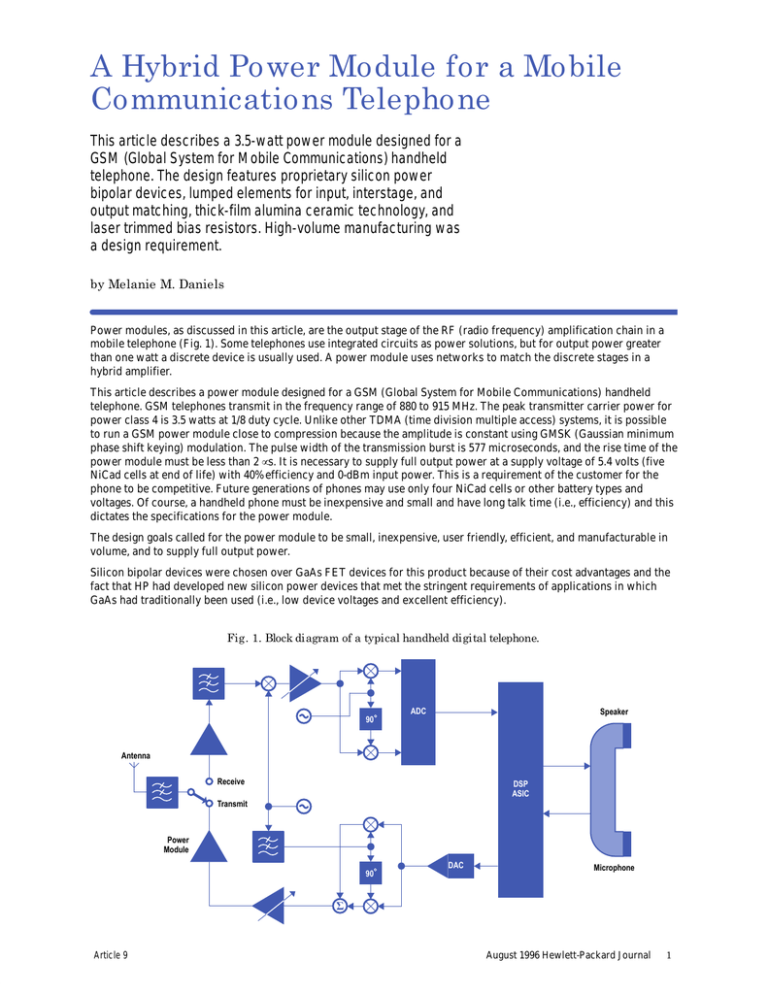
A Hybrid Power Module for a Mobile Communications Telephone This article describes a 3.5-watt power module designed for a GSM (Global System for Mobile Communications) handheld telephone. The design features proprietary silicon power bipolar devices, lumped elements for input, interstage, and output matching, thick-film alumina ceramic technology, and laser trimmed bias resistors. High-volume manufacturing was a design requirement. by Melanie M. Daniels Power modules, as discussed in this article, are the output stage of the RF (radio frequency) amplification chain in a mobile telephone (Fig. 1). Some telephones use integrated circuits as power solutions, but for output power greater than one watt a discrete device is usually used. A power module uses networks to match the discrete stages in a hybrid amplifier. This article describes a power module designed for a GSM (Global System for Mobile Communications) handheld telephone. GSM telephones transmit in the frequency range of 880 to 915 MHz. The peak transmitter carrier power for power class 4 is 3.5 watts at 1/8 duty cycle. Unlike other TDMA (time division multiple access) systems, it is possible to run a GSM power module close to compression because the amplitude is constant using GMSK (Gaussian minimum phase shift keying) modulation. The pulse width of the transmission burst is 577 microseconds, and the rise time of the power module must be less than 2 µs. It is necessary to supply full output power at a supply voltage of 5.4 volts (five NiCad cells at end of life) with 40% efficiency and 0-dBm input power. This is a requirement of the customer for the phone to be competitive. Future generations of phones may use only four NiCad cells or other battery types and voltages. Of course, a handheld phone must be inexpensive and small and have long talk time (i.e., efficiency) and this dictates the specifications for the power module. The design goals called for the power module to be small, inexpensive, user friendly, efficient, and manufacturable in volume, and to supply full output power. Silicon bipolar devices were chosen over GaAs FET devices for this product because of their cost advantages and the fact that HP had developed new silicon power devices that met the stringent requirements of applications in which GaAs had traditionally been used (i.e., low device voltages and excellent efficiency). Fig. 1. Block diagram of a typical handheld digital telephone. ADC Speaker 90 Antenna Receive DSP ASIC Transmit Power Module 90 DAC Microphone Article 9 August 1996 Hewlett-Packard Journal 1 Fig. 2. GSM power module evolution. Original Version Current Version Fig. 2 is a photograph of the power module. The schematic diagram, Fig. 3, shows the electrical design of the power module. The bias circuits must be simple and fast because of the pulsed nature of the GSM modulation. Because of the low voltage requirements, proprietary silicon power bipolar devices were developed. The collector of each stage simply has an RF choke to the 5.4V minimum supply voltage, Vcc, and a bypass capacitor to ground. The base voltage supply is used to turn the amplifier on and off and to control the output power level of the module. The control voltage, Vc, is pulsed at 1/8 duty cycle with a square wave from 0V when the module is off to 4.0V when the module supplies full output power. The base of each stage has a series resistor to the control voltage. This resistor is adjusted to compensate for each transistor’s current gain, β. This is done using active laser trimming and will be discussed as a separate topic. Since the power control voltage supplied by the phone does not have the capability of supplying the base current of each stage, a low-frequency n-p-n transistor, Q4, is used to buffer the control voltage. The collector of Q4 is biased by the supply voltage, Vcc. The base of Q4 is driven by the power control voltage and the emitter supplies the necessary voltage and current to the base of each RF stage. The RF design uses lumped elements for input, interstage, and output matching. The design requires three stages to achieve the gain requirements. The first stage is a driver stage that is class-A biased. The second and third stages are class-AB biased for efficiency. The third-stage transistor also has some internal matching within the package. The input impedance of the silicon power transistor chip is about 1.5 ohms. This must be transformed up to a larger impedance by a matching network Fig. 3. Schematic diagram of the GSM power module. Vcc (+5.4V) C10 C8 C7 C12 C6 C5 C2 RF Out R7 Q3 R6 C13 C16 Q2 1 C18 R5 C1 L C17 C15 Q1 RF In C19 Q4 Vc R2 (Laser Trimmed) R3 (Laser Trimmed) R4 (Laser Trimmed) R1 Article 9 August 1996 Hewlett-Packard Journal 2 Fig. 4. Packaged output stage transistor. Ceramic Substrate MOS Capacitors 0.001-inchDiameter Gold Wire Top View Four Single Cells In Parallel Side View that is physically as close to the chip as possible. This is achieved using a 0.001-inch-diameter bond wire as a series inductor from the base of the chip to a shunt MOS capacitor at the input of the transistor package (Fig. 4). This configuration makes a very high-Q input matching network. The exact value of capacitor and the length of bond wire had to be empirically optimized to achieve the maximum transformation within the transistor package. The most critical and sensitive part of the matching networks is the output of the final stage. High-Q lumped-element components are used in the output matching network to achieve the low losses necessary to meet the efficiency requirements. Since the design has more than 45 dB of small-signal gain in a 1-inch-by-0.5-inch package, stability and isolation were quite challenging. The placement and values of the RF chokes and decoupling capacitors were critical. Large-value capacitors could not be placed on the base bias network, since this would slow down the pulse response of the module. Mechanical Design As previously mentioned, some of the primary design goals were (1) low cost because this is a commercial product, (2) small size to allow phone manufacturers to design smaller products for portability (also a competitive advantage for HP), and (3) compatibility with high-volume manufacturing. In addition, the power module component had to be supplied as a surface mount component in tape-and-reel form. The mechanical design of the power module turned out to be one of the most challenging parts of the development project. At the time the project was started, most competitors were using soft board for the substrate material and surface mount lumped components for matching. This material definitely meets the cost criteria, but there were thermal, RF matching, and laser trimming limitations. Thick-film alumina ceramic technology was chosen for the board material. Even though the material is more expensive, this is offset by the fact that the RF matching networks are more compact because of the high dielectric constant εr = 9.1. Also, the resistors and inductors can be printed on the board, thus reducing the part count. Ceramic has superior thermal conductivity compared to soft boards. The most persuasive reason for ceramic substrates is that they do not require a metal carrier to be surface mounted. The vias in a ceramic board can be filled with metal paste so components can be placed directly on top of the via. This reduces the emitter-to-ground inductance for the transistors and gives superior gain and efficiency performance. This factor also reduces the size of the module to 1 inch by 0.4 inch. Standard surface mount components on PdAg traces are used for lumped-element matching and custom surface mount packages are used for the RF transistors. The inputs and outputs of the power module use wraparound edge vias. This is commonly referred to as an LCC (leadless chip carrier) for surface mount component manufacturers. It is inexpensive because no leadframes need to be attached. The metal thick film used in the vias must pass all solderability tests. Volume Assembly Fig. 5 shows the process flow for manufacturing the power modules. Modules are built in array form with 40 modules per 4-inch-by-4-inch array. More modules per array reduces the ceramic substrate cost and the surface mount assembly cost but also increases the complexity of substrate manufacturing. The boards are populated by a Article 9 August 1996 Hewlett-Packard Journal 3 Fig. 5. Volume assembly process flow. Fabricate Substrates (Subcontractor) Populate Board in Arrays (Subcontractor) Reflow Using No-Clean SN96 (220 C) (Subcontractor) Active Laser Trim in Arrays (Subcontractor and HP) Inspect (HP) Attach Lids in Arrays (HP) Snap Arrays into Individual Modules (HP) Test (HP) Inspect (HP) Package in Tape and Reel (HP) Ship (HP) subcontractor with standard pick-and-place equipment, then reflowed at a peak temperature of 220°C using SN96 solder paste. The high-temperature reflow was chosen to prevent a secondary reflow by the customer when the power module is surface mounted into the telephone. Developing the reflow profiles with the chosen thick-film paste and high-temperature solder was not a trivial task. The populated arrays are then actively laser trimmed. Each base bias resistor (three per module) must be trimmed with the laser to set the transistor collector current. This is to compensate for β variation in device fabrication. The simpler bias scheme was chosen because we couldn’t afford the cost and efficiency loss of an active bias circuit. Developing the laser trim process was another challenging aspect of this product. Two of the transistors are biased off (have the bases grounded) while the third is being trimmed. This is necessary to avoid oscillations caused by the high gain and the difficulty of adequate grounding while the modules are in array form. Extensive development was required to obtain good RF grounding on the backside of the module and in the bias probes while laser trimming. A grounding gasket made of silver impregnated rubber is used with a vacuum to achieve backside grounding. High-frequency probes with good 50-ohm loads are used on all inputs and outputs to avoid oscillations. Special software was developed for the laser trimmer. Algorithms were written to compensate for the current drawn through the grounded-base transistors. In addition, the resistors and transistors heat up during the trim process and this has to be compensated. The trim process has to be done in a pulsed bias mode, since the module cannot be run in CW mode without thermal runaway. Finally, the output power cannot reach saturation before the maximum control voltage is reached, since this impacts the customer’s power control loop. To resolve this issue, the modules are trimmed at a control voltage of 3.2V maximum. Article 9 August 1996 Hewlett-Packard Journal 4 Fig. 6. Single device cell. After laser trimming the lids are attached in array form. The array is then separated into individual units, which are tested using automated test equipment. All of the problems addressed for the laser trimming were also present for the automated test process. The module grounding is absolutely critical to testing RF parameters. Developing test fixtures that could test hundreds of modules per hour, three shifts a day, and still retain a good RF ground was critical to the success of the product. The average test time per module is 20 seconds. The automated test programs are complex because of the number of tests that have to be performed and the fact that they all have to be done in pulsed mode. Transistor Modeling Transistor modeling was used to develop linear and nonlinear device models for a single cell of the transistor used in the power module. These building blocks were then used to model the entire power module. The modeling effort included correlating measured device data with the models and modifying the models when necessary. The HP Microwave Design System was used for the linear and nonlinear modeling of the device and the package. The first step was to use parameter extraction techniques to get a Gummel-Poon SPICE model1 of the single-cell device. Next, models were developed for the packages. To make low-voltage bipolar transistors, many new processes were used. These devices have fine geometry to achieve the higher gain necessary for talk-time efficiency. This changed many of the model parameters traditionally used for silicon power transistors. The single device chosen for modeling actually consists of four separate quarter cells on each device as shown in Fig. 6. Each quarter cell has 40 emitter fingers with each finger having an approximate capacity of 2 mA of continuous current. With the existing technology it was not possible to extract the parameters of the entire device with 160 fingers and a maximum current of 360 mA, so the quarter cell with 40 fingers was used for the parameter extraction. These devices have HP proprietary epitaxial material and geometries. The device was placed into the standard 86 package shown in Fig. 7 for the second stage of the power module. This is a plastic encapsulated package used for high-volume manufacturing and low power dissipation. The output stage has a custom package as shown in Fig. 4. Thermal dissipation is not a major issue in our application because of the 12.5% duty cycle pulsed operation. The Ebers-Moll model2,3 is a good general-purpose model, but is not sufficient over wide regions of operation because of approximations in the equations. The Gummel-Poon model1 takes second-order effects into account and gives more accurate results. The model we used is a modified Gummel-Poon model.4 The n-p-n transistor dc and ac circuits are shown in Figs. 8 and 9 respectively. Among the second-order effects included in the Gummel-Poon model is junction capacitance in the emitter, base, and collector. The Ebers-Moll model holds these capacitances constant but they are more accurately modeled in the Gummel-Poon model as functions of junction voltage. A total of nine model parameters are needed to model the junction capacitance accurately.5 Finite resistance and the effects of surfaces, high current injection, and nonideal diodes make the collector and base current vary nonuniformly with base-to-emitter voltage. These effects are modeled using two diodes. Article 9 August 1996 Hewlett-Packard Journal 5 Fig. 7. Standard 86 package. 0.51 (0.020) 4 CL 1 3 2.43 (0.107) 1.96 (0.077) 2 3.05 (0.120) 2.16 (0.085) CL 2.16 (0.085) 1.77 (0.070) 1.27 (0.050) 0.66 (0.026) 0.25 (0.010) 0.15 (0.006) Dimensions are in millimeters (inches). Fig. 8. Modified Gummel-Poon n-p-n dc model. Qc2 Qc1 lb lbr Rbb Base lc Rc llc Collector Qcs Substrate lle lbf lcf lcr Qe E Re Emitter Another complex second-order effect is the variation of unity-gain bandwidth, fT, with Ic and Vce. At low currents, fT is almost totally dependent on the gm of the device and the junction capacitance.5 At moderate currents, the diffusion capacitance at the base-emitter and base-collector junctions starts to cancel any increase in gm, which causes fT to remain constant. This is the constant transit time region. At high currents, the forward transit time of the transistor increases because of space charge limited current flow, which leads to base widening and two-dimensional injection effects. All of the parameters of the modified Gummel-Poon model are extracted using a modeling system developed by HP. Complete and accurate model parameter sets can be obtained in about two hours using Hewlett-Packard’s test system, Article 9 August 1996 Hewlett-Packard Journal 6 Fig. 9. Modified Gummel-Poon n-p-n ac model. Qc2 Cu Rbb Qu Base Rc Collector Qm Qpi Cpi Go Css Substrate Re Emitter test and modeling software, and new modeling methods.6 A through-reflect-line (TRL) calibration method is used and the fixture and bond wires to the device are completely characterized and deembedded to get an accurate model of the device alone. At the time this work was completed, it was not possible to measure large transistors because of the limitations of the dc power supplies and thermal dissipation problems. To overcome this difficulty, one quarter of the cell was extracted. This was possible since there was a small quarter-cell test transistor on the original engineering wafer as shown in Fig. 10. The Gummel-Poon SPICE file that was obtained by HP’s parameter extraction software of this quarter cell is shown in Fig. 11. The schematic for the SPICE file can be seen in Fig. 12. Since this work was completed, HP has developed a pulsed parameter extraction system that can measure power transistors and a power Gummel-Poon model is being developed to compensate for thermal considerations. With the basic model obtained previously, however, the model for the entire device was developed on the HP Microwave Design System by paralleling four of the quarter cells as shown in Fig. 13. The quarter cell has one base and one emitter pad as shown previously in Fig. 10. The entire cell has one base pad for all four cells and one emitter pad for two cells as shown in Fig. 6. This must be compensated in the models. The parameter extraction SPICE file (Figs. 11 and 12) clearly shows the capacitance of both the base and emitter pads, CPADBC and CPADEC, respectively. The two-emitter-pad capacitance and the one-base-pad capacitance are added to the model of the four parallel quarter cells (Fig. 13) as components CMP103 and CMP106. This file is the basis for the models of the full device. Separately, similar parameter extraction methods were performed to model the 86 package and the custom output stage package. The 86 package has been modeled extensively for use with other products and can be found in the HP Components Data Book.7 The HP Microwave Design System package model for the 86 package is shown in Fig. 14. Fig. 10. Quarter device cell. Article 9 August 1996 Hewlett-Packard Journal 7 Fig. 11. Quarter-cell SPICE parameter extraction output. .SUBCKT melanie 1 2 3 LE 3 4 3E-10 LB 2 5 6E-10 CFIXBE 2 3 1E-14 CFIXBC 2 1 3E-14 CFIXEC 1 3 2E-13 CPADBC 5 1 4.1E-13 CPADEC 4 1 4.1E-13 Q1 1 5 4 NPN + AREA = 1 .MODEL NPN NPN + IS = 3.598E-15 + BF = 280.7 + NF = 0.9935 + VAF = 33.16 + IKF = 299.9 + ISE = 9.91E-11 + NE = 2.399 + BR = 54.61 + NR = 0.9886 + VAR = 1.511 + IKR = 81 + ISC = 8.674E-13 + NC = 1.587 + RB = 0.752 + IRB = 0 + RBM = 0 + RE = 2.448 + RC = 1.228 + XTB = 0 + EG = 1.11 + XTI = 3 + CJE = 5.055E-12 + VJE = 1.148 + MJE = 0.5965 + TF = 1.6E-11 + XTF = 0.006656 + VTF = 0.02785 + ITF = 0.001 + PTF = 23 + CJC = 1.352E-12 + VJC = 0.4776 + MJC = 0.2508 + XCJC = 0.001 + TR = 1E-09 + FC = 0.999 .ENDS Fig. 12. Quarter device cell schematic of the SPICE file. Collector CFIXBC CPADBC 1 LB 2 Base CPADEC 5 CFIXEC 4 LE CFIXBE 3 Emitter Article 9 August 1996 Hewlett-Packard Journal 8 Fig. 13. HP Microwave Design System model for a full single cell. CMP103 C = 0.41 pF CMP69 NPNBJT CMP106 C = 0.82 pF CMP68 NPNBJT CMP67 NPNBJT 1 2 CMP65 NPNBJT L = 0.01 nH 3 CMP102 Fig. 14. Simplified HP Microwave Design System model of the second-stage transistor in the 86 package. CMP6 CMP7 CMP11 Out L = L3 C = CCB CMP10 CMP8 CMP2 In L = L1 L = LB Z = Z1 L = D1 V = V1 R=0 G= 0 F =0 Basic 1 Die CMP3 CMP5 C = CEB Z = Z3 L = D3 V = V3 R=0 G= 0 F =0 2 3 L = LE CMP4 Z = Z2 L = D2 V = V2 R=0 G= 0 F =0 C = CEC CMP9 CMP12 L = L2 GND Article 9 August 1996 Hewlett-Packard Journal 9 Both of these models were used for linear and nonlinear designs of the power module. Agreement between the measured performance and the simulated performance was excellent for the linear design (within ±0.5 dB of gain) and good for the nonlinear design (within ±2 dBm of the 1-dB compression point). The performance of the models was good because this was a pulsed application and deviations because of thermal considerations were not a factor. Results The GSM power module was engineering released in November 1993 and manufacturing released in May 1994. Over one million of the original GSM power module have been shipped and the module has since gone through two design upgrades to smaller and leadless modules to satisfy customer redesign needs. We now have a manufacturing line and processes that are being used for new products. The module has been a success in the power cellular market. Project Management and Acknowledgements This was and is a global project. The customers and sales offices are in Europe and the wafer fab is in Newark, California. The marketing team was originally in San Jose, California, the R&D team was in Folsom, California, and the manufacturing team was in Malaysia and Folsom. We had never worked together before and there were large learning curves. HP’s Malaysia operation had never manufactured a product using thick-film surface mount technologies with the complex RF testing and active laser trimming required. The engineering team had never designed a product for these high volumes. Communication and project management were critical. Many hours were spent on the phone, in meetings, writing email, and traveling. I would like to acknowledge Hanan Zurkowski, Thomas Franke, Rich Levitsky, Mark Dunn, the power module groups in Folsom and Malaysia, and the field sales team for their contributions to the success of this project. References 1. H.K. Gummel and H.C. Poon, “An Integral Charge Control Model of Bipolar Transistors,” Bell System Technical Journal, May-June 1970, pp. 827-852. 2. R. Pierret, Modular Series on Solid State Devices, Volumes I and II, Addison-Wesley Publishing Company, 1983. 3. I. Getreu, “Modeling the Bipolar Transistor, A New Series,” Electronics, September 19, 1974, pp. 114-120. 4. HP 94453A-UCB Bipolar Transistor Model and Parameter Extraction, Section 5, Hewlett-Packard Company, 1993. 5. I. Getreu, “Modeling the Bipolar Transistor, Part 2,” Electronics, October 31, 1974, pp. 71-75. 6. M. Dunn, “Device Model and Techniques for Fast Efficient Nonlinear Parameter Extraction of BJT Devices,” The HPEEsof High-Frequency Modeling and Simulation Seminar, Hewlett-Packard Company, 1994. 7. Communication Components Catalog—GaAs and Silicon Products, Hewlett-Packard Company, 1993. Bibliography 1. G. Gonzalez, Microwave Transistor Amplifiers, Prentice-Hall, 1984. 2. Simulating Highly Nonlinear Circuits using the HP Microwave and HP RF Design Systems, Application Note 85150-2, Hewlett-Packard Company, 1993. 3. T.K. Ishii, Microwave Engineering, Harcourt Brace Jovanovich, 1989. 4. P.W. Tuinenga, SPICE, A Guide to Circuit Simulation and Analysis Using PSPICE, Prentice-Hall, 1992. Article 9 Go to Article 10 Go to Table of Contents Go to HP Journal Home Page August 1996 Hewlett-Packard Journal 10

