Implementation of Current Reuse Structure in Radio Frequency System
advertisement
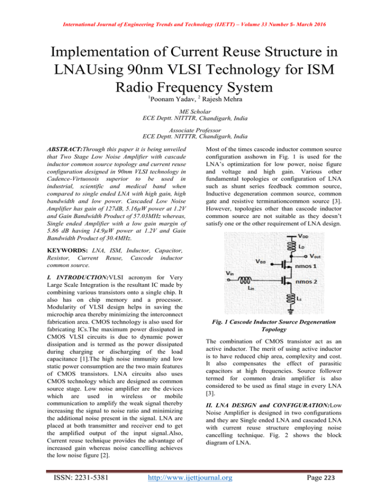
International Journal of Engineering Trends and Technology (IJETT) – Volume 33 Number 5- March 2016 Implementation of Current Reuse Structure in LNAUsing 90nm VLSI Technology for ISM Radio Frequency System 1 Poonam Yadav, 2 Rajesh Mehra ME Scholar ECE Deptt. NITTTR, Chandigarh, India Associate Professor ECE Deptt. NITTTR, Chandigarh, India ABSTRACT:Through this paper it is being unveiled that Two Stage Low Noise Amplifier with cascade inductor common source topology and current reuse configuration designed in 90nm VLSI technology in Cadence-Virtuosois superior to be used in industrial, scientific and medical band when compared to single ended LNA with high gain, high bandwidth and low power. Cascaded Low Noise Amplifier has gain of 127dB, 5.16µW power at 1.2V and Gain Bandwidth Product of 57.03MHz whereas, Single ended Amplifier with a low gain margin of 5.86 dB having 14.9µW power at 1.2V and Gain Bandwidth Product of 30.4MHz. Most of the times cascode inductor common source configuration asshown in Fig. 1 is used for the LNA’s optimization for low power, noise figure and voltage and high gain. Various other fundamental topologies or configuration of LNA such as shunt series feedback common source, Inductive degeneration common source, common gate and resistive terminationcommon source [3]. However, topologies other than cascode inductor common source are not suitable as they doesn’t satisfy one or the other requirement of LNA design. KEYWORDS: LNA, ISM, Inductor, Capacitor, Resistor, Current Reuse, Cascode inductor common source. I. INTRODUCTION:VLSI acronym for Very Large Scale Integration is the resultant IC made by combining various transistors onto a single chip. It also has on chip memory and a processor. Modularity of VLSI design helps in saving the microchip area thereby minimizing the interconnect fabrication area. CMOS technology is also used for fabricating ICs.The maximum power dissipated in CMOS VLSI circuits is due to dynamic power dissipation and is termed as the power dissipated during charging or discharging of the load capacitance [1].The high noise immunity and low static power consumption are the two main features of CMOS transistors. LNA circuits also uses CMOS technology which are designed as common source stage. Low noise amplifier are the devices which are used in wireless or mobile communication to amplify the weak signal thereby increasing the signal to noise ratio and minimizing the additional noise present in the signal. LNA are placed at both transmitter and receiver end to get the amplified output of the input signal.Also, Current reuse technique provides the advantage of increased gain whereas noise cancelling achieves the low noise figure [2]. ISSN: 2231-5381 Fig. 1 Cascode Inductor Source Degeneration Topology The combination of CMOS transistor act as an active inductor. The merit of using active inductor is to have reduced chip area, complexity and cost. It also compensates the effect of parasitic capacitors at high frequencies. Source follower termed for common drain amplifier is also considered to be used as final stage in every LNA [3]. II. LNA DESIGN and CONFIGURATION:Low Noise Amplifier is designed in two configurations and they are Single ended LNA and cascaded LNA with current reuse structure employing noise cancelling technique. Fig. 2 shows the block diagram of LNA. http://www.ijettjournal.org Page 223 International Journal of Engineering Trends and Technology (IJETT) – Volume 33 Number 5- March 2016 INPUT LNA WITH CURRENT REUSE STRUCTURE NOISE CANCELLING NETWORK OUTPUT NETWOR K provides high output impedance and better input to output isolation. The resistor and inductor combined to form bias circuit. The large value of resistor represents high impedance which blocks the AC signal to flow towards bias circuit. On the other hand, large capacitor value gives ideal AC ground for 2nd stage of amplifier [4]. Fig. 4 represents the two stage cascaded low noise amplifier. Fig. 2 LNA Block Diagram Single Ended LNA: Single ended topology includes biased cascaded transistor and output matching inductor. The function of cascade transistor is to increase output gain and matching inductor is to maximize the output power transfer and gain at fr(resonant frequency). It has the advantage of control over real part input impedance value by choosing the inductance. Biased transistor forms transistor to work as current mirror.The circuit diagram of single ended low noise amplifier is shown in Fig. 3. Fig. 4 Cascaded LNA Fig. 3 Single ended LNA Two Stage CS LNA (with Current reuse configuration):In this topology, noise cancelling technique is employed with current reuse strategy which aims to cancel the term that represents the noise figure at input transistor by identifying the nodes at which opposite polarity signal but same polarity noise appears. Now their voltages can be appropriately scaled and summed up resulting incancellation of noise and addition of the signal component. In noise cancelling criteria, the noise from 1st CS stage and 2nd CS stage both in opposite phase to each other coming to the output node of noise cancelling network. Thus reduced noise figure can be achieved. Here, the concept of using current reuse configuration is to achieve low power and it means to reprocess the bias current such that more than one stage can use it. The main problem with CMOS transistor is its implicitly low transconductance thus providing low gain. Cascaded/Differential LNA have greater availability of output swing through which power dissipation can be reduced. It provides linearity by cancellation of even order harmonics. Differential input provides improved power supply rejection ratio and common mode rejection ratio. Along with this it also gives better immunity to coupled EMI. It even uses pre-distortion techniques to reduce odd harmonics. The technique that helps in increasing the linearity of radio transmitter amplifier is called pre-distortion technique as non-linearity results in interference. III. LNA in ISM System:ISM stands for industrial, scientific and medical. These are the parts of radio spectrum which are set aside for internationally for use of RF energy for industrial, scientific and medical applications over telecommunications. They includes RF heating process, ovens and diathermy machines for muscles relaxation. Such ISM devices are used in industries for plastic welding. Since for successful operations these ISM devices should be free from noise and interferences therefore use of LNA comes into play as shown in Fig. 5 and can be used to provide low noise signals for ISM band system.The operating frequency of ISM bands is 2.4GHz. For good circuit stability it is essential to have cascade amplifier as it is mainly responsible for overall gain of LNA. Apart from this it also ISSN: 2231-5381 http://www.ijettjournal.org Page 224 International Journal of Engineering Trends and Technology (IJETT) – Volume 33 Number 5- March 2016 Fig. 8 Transient Analysis of Single Ended LNA Fig. 5 Use of LNA for ISM Band IV. RESULTS & DISCUSSION:On comparing simulation of single ended LNA with Cascaded LNA shows that former is inferior to the latter as the latter one provides high gain, low power and high bandwidth but it has high settling time. The AC analysis is being depicted in Fig. 9. When inductors are shorted and capacitors are kept open circuited then DC operating points can be determined and it is called DC Analysis shown in Fig. 10. These operating points are sometimes considered to be the equilibrium points. Simulation of Single Ended LNA:Fig. 6 depicts the single ended circuit diagram simulated in Cadence Virtuoso. Fig. 9 AC Analysis Fig. 6 Single Ended LNA in Cadence The noise coming at the output as shown in Fig. 7 is being removed by the use of noise cancelling network and the resulting transient analysis is shown in Fig. 8 which gives amplified and reduced noise signal. Fig. 10 DC Analysis It has gain margin of 5.86dB and phase margin of 87.01º as shown in Fig. 11. Fig. 11 Gain and Phase Margin Simulation of Cascaded LNA:Fig. 12 depicts the Cascaded circuit diagram again simulated in Cadence Virtuoso. Fig. 7 Noise in output signal ISSN: 2231-5381 http://www.ijettjournal.org Page 225 International Journal of Engineering Trends and Technology (IJETT) – Volume 33 Number 5- March 2016 Fig. 16 DC Analysis Fig. 12 Circuit Diagram of Cascaded LNA Again, in case of cascaded LNA noise cancelling network is being applied so as to remove the noise from the signal as shown in Fig. 13 and Fig. 14 gives the transient analysis without noise and thus being amplified. The two stages low noise amplifier has high gain margin of 127dB and phase margin of 114º and it can be seen in Fig. 17. Fig. 17 Gain & Phase Margin Now the comparison between Single Ended & Cascaded LNA both designed in 90nm VLSI technology is shown in Table 1 which reveals the better performance parameters of the second configuration. The comparison is done on the basis of settling time, gain- bandwidth product, gain margin, gain bandwidth, power and phase margin. Fig. 13 Noise signal I Table1.Comparison between the configurations S.No. Parameters 1. 2. 6. Technology No. of Transistors Settling Time Gain Margin Gain Bandwidth Power 7. GBWP Fig. 14 Transient Analysis of Cascaded LNA AC analysis shown in Fig. 15 is being done so as to get the frequency domain of the signal for calculating the ac gain and phase margin which thereby gives the gain, bandwidth and gainbandwidth product. Through AC analysis the small signal response of a circuit can also be calculated. The cascaded LNA has DC analysis as shown in Fig. 16. Fig. 15 AC Analysis ISSN: 2231-5381 3. 4. 5. Single Ended LNA 90nm 4 Cascaded LNA 5.7ps 38ns 5.86dB 34MHz 127dB 55.49MHz 14.9µW 5.16µW 30.4MHz 57.03MHz 90nm 7 V. CONCLUSION: On the basis of above simulations it can be concluded that Cascaded LNA has better resulting parameters as compared to Single ended LNA for its usage in ISM bands system. Here, high gain is achieved with the usage of current reuse structure with reduced noise http://www.ijettjournal.org Page 226 International Journal of Engineering Trends and Technology (IJETT) – Volume 33 Number 5- March 2016 technique. Also, phase margin of 114º is achieved in cascaded LNA thereby increasing the stability of the circuit. It has high output impedance of 29.7MΩ. Only the settling time in case of cascaded one is high i.e. 38ns and 5.7ps in case of single ended. VI. REFERENCES: [1] Anjali Sharma, Rajesh Mehra, “Area and Power Efficient CMOS Adder Design by Hybridizing PTL & GDI Technique.” International Journal of Computer Applications, Vol. 66, 2013, pp. 15-22. [2] GholamrezaKarimi, Saeed Haghiri, “A High Gain CMOS Low Noise Amplifier for 3.6GHz Applications using CurrentReuse Topology and Noise Cancelling Technique”, Vol. 2, 2014, pp. 174-182. [3] A. Hameed, Ali Oudah, “Improved Design of Low Noise Amplifier”, International Journal of Multimedia & Ubiquitous Engineering, Vol. 10, 2015, pp. 255-264. [4] Ritika, Rekha Yadav and VarshaSinghal, “Comparative Analysis of CMOS Low Noise Amplifier in 45nm VLSI Technology”, International Journal of Science and Advance Research in Technology, Vol. 1, 2015, pp. 110-116. ISSN: 2231-5381 http://www.ijettjournal.org Page 227
