A CMOS Power Efficient Analog Integrated Circuits for Neural Signal Acquisition
advertisement
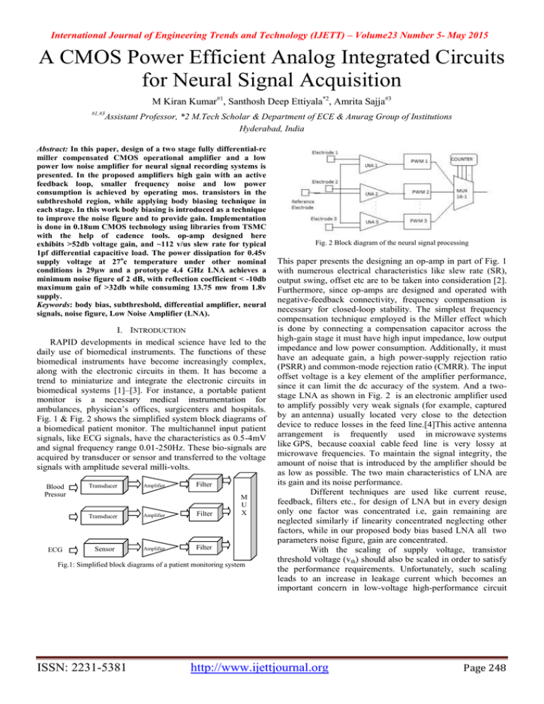
International Journal of Engineering Trends and Technology (IJETT) – Volume23 Number 5- May 2015 A CMOS Power Efficient Analog Integrated Circuits for Neural Signal Acquisition M Kiran Kumar#1, Santhosh Deep Ettiyala*2, Amrita Sajja#3 #1,#3 Assistant Professor, *2 M.Tech Scholar & Department of ECE & Anurag Group of Institutions Hyderabad, India Abstract: In this paper, design of a two stage fully differential-rc miller compensated CMOS operational amplifier and a low power low noise amplifier for neural signal recording systems is presented. In the proposed amplifiers high gain with an active feedback loop, smaller frequency noise and low power consumption is achieved by operating mos. transistors in the subthreshold region, while applying body biasing technique in each stage. In this work body biasing is introduced as a technique to improve the noise figure and to provide gain. Implementation is done in 0.18um CMOS technology using libraries from TSMC with the help of cadence tools. op-amp designed here exhibits >52db voltage gain, and ~112 v/us slew rate for typical 1pf differential capacitive load. The power dissipation for 0.45v supply voltage at 27oc temperature under other nominal conditions is 29µw and a prototype 4.4 GHz LNA achieves a minimum noise figure of 2 dB, with reflection coefficient < -10db maximum gain of >32db while consuming 13.75 mw from 1.8v supply. Keywords: body bias, subthreshold, differential amplifier, neural signals, noise figure, Low Noise Amplifier (LNA). I. INTRODUCTION RAPID developments in medical science have led to the daily use of biomedical instruments. The functions of these biomedical instruments have become increasingly complex, along with the electronic circuits in them. It has become a trend to miniaturize and integrate the electronic circuits in biomedical systems [1]–[3]. For instance, a portable patient monitor is a necessary medical instrumentation for ambulances, physician’s offices, surgicenters and hospitals. Fig. 1 & Fig. 2 shows the simplified system block diagrams of a biomedical patient monitor. The multichannel input patient signals, like ECG signals, have the characteristics as 0.5-4mV and signal frequency range 0.01-250Hz. These bio-signals are acquired by transducer or sensor and transferred to the voltage signals with amplitude several milli-volts. Blood Pressur e ECG Transducer Amplifier Filter Transducer Amplifier Filter Sensor Amplifier Filter M U X Fig.1: Simplified block diagrams of a patient monitoring system ISSN: 2231-5381 Fig. 2 Block diagram of the neural signal processing This paper presents the designing an op-amp in part of Fig. 1 with numerous electrical characteristics like slew rate (SR), output swing, offset etc are to be taken into consideration [2]. Furthermore, since op-amps are designed and operated with negative-feedback connectivity, frequency compensation is necessary for closed-loop stability. The simplest frequency compensation technique employed is the Miller effect which is done by connecting a compensation capacitor across the high-gain stage it must have high input impedance, low output impedance and low power consumption. Additionally, it must have an adequate gain, a high power-supply rejection ratio (PSRR) and common-mode rejection ratio (CMRR). The input offset voltage is a key element of the amplifier performance, since it can limit the dc accuracy of the system. And a twostage LNA as shown in Fig. 2 is an electronic amplifier used to amplify possibly very weak signals (for example, captured by an antenna) usually located very close to the detection device to reduce losses in the feed line.[4]This active antenna arrangement is frequently used in microwave systems like GPS, because coaxial cable feed line is very lossy at microwave frequencies. To maintain the signal integrity, the amount of noise that is introduced by the amplifier should be as low as possible. The two main characteristics of LNA are its gain and its noise performance. Different techniques are used like current reuse, feedback, filters etc., for design of LNA but in every design only one factor was concentrated i.e, gain remaining are neglected similarly if linearity concentrated neglecting other factors, while in our proposed body bias based LNA all two parameters noise figure, gain are concentrated. With the scaling of supply voltage, transistor threshold voltage (vth) should also be scaled in order to satisfy the performance requirements. Unfortunately, such scaling leads to an increase in leakage current which becomes an important concern in low-voltage high-performance circuit http://www.ijettjournal.org Page 248 International Journal of Engineering Trends and Technology (IJETT) – Volume23 Number 5- May 2015 designs. Multiple thresholds can be used to deal with the leakage problem in low-voltage high-performance CMOS circuits. This technique has commonly been used in DRAM chips by raising threshold voltages of the array devices with a fixed body bias [5]. However, only the standby leakage power can be reduced and the large inserted MOSFET’s will increase the area and delay. Moreover, the data retention must also be considered [18]. The remainder of the paper is organized as follows. Section II describes the circuit implementation of the Operational amplifier. Section III describes the circuit implementation of the LNA. Section IV discusses the measurement results, and Section V presents the conclusion. II. DESIGN OF OPERATIONAL AMPLIFIER Differential amplifier is one of the most important circuits in analog design domain. As the name indicates that only processes the difference between the two input signals. It cancels out the common voltage applied to both inputs. But, practically there always exists some amount of common voltage both at the inputs. As it cancels most of the common voltage at the input hence, noise and bias voltages are cancelled out. Single Ended Differential Amplifier is considered where two inputs with one output is provided, an ideal op-amp having a single ended output is characterized by a differential input, infinite voltage gain, infinite input resistance and zero output resistance. Where the is the transconductance of NMOS input transistor M1 or M2 and is transconductance of PMOS transistor M6 and gm7 is the transconductance of NMOS transistor M7 (5) (6) Where the R02 and R04 are the output resistances M2 and M4, whereas the R06 and R07 are the output resistances M6 and M7 transistors Further analysis tells that gm is a function of device dimension (W/L), bias current (ID) and overdrive voltage (Vov).It is also a function of process parameters e.g. oxide capacitance Cox and mobility of electrons µn. The designers generally do not have control over Cox and µn. In a practical op-amp however these characters cannot be generated but their performance will be sufficiently good for the circuit behaviour to closely approximate the characters of an ideal op-amp in most of the applications. Fig. 4 schematic diagram of differential amplifier Fig. 3 General Two stage CMOS Op-amp Biasing Circuit The DC gain for a multistage Op-amp is given as (1) Where Av1 or Av2 are gains of two different stages and can be represented in following form (2) Here Av is DC gain of Amplifier system independent from the frequency, Gm is transconductance of input network and Rout is the effective output resistance of output network. The complete circuit analysis tells us that Various techniques are available for biasing the transistors in the IC technology. Previously it was the voltage biasing which was primarily in use, but presently it is the current biasing is widely used due to its several advantages. MOS devices when operate in saturation region, their current is almost constant (neglect lambda effect). A voltage generally produces flow of electron in a material (metal and semiconductor). Same way when a current flows through a material it produces voltage across it. This concept is the core of current mirror circuits shown in Fig. 5 (3) (4) ISSN: 2231-5381 http://www.ijettjournal.org Page 249 International Journal of Engineering Trends and Technology (IJETT) – Volume23 Number 5- May 2015 Fig. 5 Current Mirror circuit This input differential transconductance stage that forms the input of the op amp this first stage of an op-amp due to their differential input to single ended output conversion and their high gain. The Gain of the single ended differential amplifier is given as: When coming part to the second stage Fig. 6 which is a gain stage which is given as Fig. 7 Level shifter and buffer circuit Any input sources which are connected to ground are automatically referenced to the center of the supply voltage, so the output voltage is automatically referenced to the ground. Single supply systems do not have the convenient ground reference that of dual supply systems have, thus biasing must be employed to ensure that the output voltage swings. Bias circuit is provided in order to establish the operating point of each transistor in their quiescent stage. For a transistor to work as a constant current source in weak inversion, VDS > 3VT. Thus the current flowing can be given as: And the trans conductance is provided as: Fig. 6 Second Stage circuit This common source second stage increase the DC gain by an order of magnitude and also maximizes the output signal swing for the provided supply voltage. This makes an important role in reducing the power consumption [6, 7]. The Gain of second stage can be given as: Level shifter used to convert one voltage signal level to other voltage level signal and this is more significant circuit component in VLSI systems. In order to provide low resistance load the second stage must be followed with an buffer circuit Fig. 7. The Buffer circuit main objective is to lower the output resistance and maintain large signal swing [8, 9]. For the two-stage op amp, the simplest compensation technique is to connect a capacitor across the high gain stage, this results in the pole splitting phenomena which improves the closed loop stability significantly. however, due to the feed forward path through the Miller Capacitor, a right half plane zero will also created, which can be nullified by using current buffer compensation in series with the compensation capacitor. An uncompensated right half plane zero radically reduces the maximum achievable gain-bandwidth product, since it makes a negative phase contribution to the open-loop gain at a relatively high frequency [10]. Op Amps used exhibit a large-signal behaviour called ―slewing‖. Thus Slew rate states that the rate of change of output voltage with respective to time for a step change at an input which can also be depicts that the maximum rate at which the capacitive load is charged and discharged. The slew rate is thus defined as III. PROPOSED LOW NOISE AMPLIFIER To design low noise amplifiers which play a key role in receivers. In general, in a receiver which is composed of several blocks in cascade, the first block has the dominant role on the noise performance of the systems and for the blocks ISSN: 2231-5381 http://www.ijettjournal.org Page 250 International Journal of Engineering Trends and Technology (IJETT) – Volume23 Number 5- May 2015 that are farther from the antenna, their noise contribution is attenuated by the gain of their preceding stages. Similar to Friis equation [11] for noise performance, one may conclude that the effect of blocks following the LNA in the chain is more pronounced in the overall gain of the system as they experience a larger input signal. Fig. 9 First stage LNA Fig. 8 Block diagram of low noise amplifier The block diagram of low noise amplifier can be as shown in Fig. 8 which consists of two stages S1 and S2 where in S1 noise figure is concentrated and while in S2 gain improvisation is done. Here body bias concept is used in both stages for noise figure decrement and gain maximisation it can be explained in detail in further sections. Noise Figure: Noise figure (NF) is a measure of signal-to-noise ratio (SNR) degradation as the signal traverses the receiver front-end. Mathematically, NF is defined as the ratio of the input SNR to the output SNR of the system. NF = SNRin SNRout Body Bias : Body bias involves connecting the transistor bodies to a bias network in the circuit layout rather than to power or ground. The body bias can be supplied from an external (offchip) source or an internal (on-chip) source. In the on-chip approach, the design usually includes a charge pump circuit to generate a reverse body bias voltage and/or a voltage divider to generate a forward body bias voltage. Reverse body bias, which involves applying a negative body-to-source voltage to an n-channel transistor, raises the threshold voltage and thereby makes the transistor both slower and less leaky. Forward body bias, on the other hand, lowers the threshold voltage by applying a positive body-to-source voltage to an nchannel transistor and thereby makes the transistor both faster and leakier. The polarities of the applied bias described above are the opposite for a p-channel transistor. The two stages can be explained in detail as below as improving noise figure in stage 1 and in stage 2 gain of amplifier is increased. A. Improving noise figure using body bias In the schematic we can observe that in two stage LNA cascode amplifiers (combination of common source and common gate) are used in cascade combination and reason for selecting cascode amplifier as LNA is as it has good reverse isolation and it can be as follow ISSN: 2231-5381 As shown in Fig. 9 the cascode amplifier is used with a source de generation and a series gate inductor is used for input and noise impedance matching [12] [13]. In this stage circuit is biased by a current source and a capacitor has been added in parallel with the current source to attenuate its noise. The reason for such biasing scheme is that when continuous varying of bias or bulk voltage it may affect the dc characteristics of transistor to avoid such condition current source is used and capacitor placed parallel will avoid noise caused by current source. Fig. 10 Noise model of a transistor in the first stage of a LNA The different sources of noises at high frequencies can be as channel thermal noise and gate induced noise and the noise model can be shown in Fig. 10[14] [15] can be used for a MOS transistor in which i2nd is the power spectral density (PSD) of the channel thermal noise,i2ng is the PSD of the gateinduced noise, gg is the conductance of a gate resistance utilized for modelling the effect of gate-induced noise. Rs is the resistance of the voltage source which drives the transistor and Cgs is the gate-source capacitance of the MOS transistor. The bulk resistance is another source of noise in MOS transistors. Note that the noise associated with this resistance cannot be avoided even if the bulk and source terminals of the MOS device are shorted together [16]. This is due to the fact that there is a distance between the bulk contacts and the physical bulk node. The bulk resistance is a distributed resistance, and thus it is typically difficult to quantitatively calculate its contribution to the noise of the MOS transistor [16]. Fig. 11 shows the noise equivalent model of the MOS transistor when bulk resistance noise is taken into account. As can be seen from this figure, if we denote the equivalent noise resistance of the distributed bulk resistance as RB, its PSD would be Vnb2 = 4kTRB f which http://www.ijettjournal.org Page 251 International Journal of Engineering Trends and Technology (IJETT) – Volume23 Number 5- May 2015 appears as a noise voltage source at the bulk terminal. Based on Fig. 11, to refer this noise source to the drain terminal of the MOS transistor, its PSD is multiplied by gmb2. Inb2 = 4kTRB gmb2 f [20] As shown in Fig. 9 body biasing at the first stage of LNA which is reserved for improvement of noise figure, is applied to the CS transistor and not to the CG transistor. The reason for this is the fact that cascode amplifier is a cascade combination of a CS and a CG amplifier. As discussed before, in a cascade configuration, the effect of noise figure of the first stage is dominant over that of the other stages. Therefore, here in a cascode configuration, the effect of noise figure of the CS stage is dominant over that of the CG stage and body biasing is only applied to the CS stage. However, if the bulk voltage of the CS transistor is varied, its dc parameters will also change. This is because by changing the bulk voltage, threshold voltage of the transistor changes according to: Fig. 11 Noise model of a MOS transistor in the first stage of an LNA including the effect of bulk resistance noise. Considering the fact that this noise source is not correlated to the channel thermal noise and gate-induced noise, its PSD is simply added to the PSD calculated for the output current noise at the drain terminal of MOS transistors in Therefore, to decrease the contribution of the bulk resistance noise component on the overall noise performance of the MOS transistor, it is desirable to decrease the value of in g mb. The equation for gmb is From the above equation it is very clear that by varying gm all different noises can be decreased and it can be done by varying source to bulk voltage i.e., VSB, so by decreasing bulk voltage (V1) from Fig. 9 i.e., connecting V1 in reverse bias by which VSB increases trans conductance gm decreases automatically noise due to different causes decreases by which noise figure also decreases. In addition to these a small part of short noise also added to overall PSD and it can be as described as white noise .The PSD of the shot noise is proportional to the current of p-n junction and is given by Ind2 = 2qID f in which q is the charge of electron and ID is the current in the p-n junction[20]. Thus, in the presence of shot noise and considering its independence from other noise sources of the transistor is revised to Where Vth0 is the threshold voltage of the transistor when its bulk-source voltage is zero, i.e., VBS=0V. This in turn means that, changing the bulk voltage to control the noise figure results in changing the operation point of the LNA, an effect which is not desirable. As a solution to this problem, the first stage is biased with a current source (rather than a voltagebiasing). In order to minimize any leakage of noise of the current source devices into the LNA, a large capacitor is added in parallel with the current source to provide a lowimpedance path for the noise to ground. Gain maximisation using body bias The second stage deals with improvisation of gain of amplifier and the schematic of second stage can be as shown in Fig. 12, as we know for every amplifier gain should be maximum and as it is a low noise amplifier there will be a trade of between noise figure and gain so by compromising gain, noise figure is improved and finally we should make both parameters in balance such that system should not deviate from its behaviour. To cover a wide dynamic range, the gain of the receiver should be adjusted in accordance with the power level of the input signal. Fig. 12 Second stage LNA In other words, for a small input signal the gain should be large and for a large input signal the gain should be small to avoid the saturation of the subsequent receiver chain ISSN: 2231-5381 http://www.ijettjournal.org Page 252 International Journal of Engineering Trends and Technology (IJETT) – Volume23 Number 5- May 2015 blocks. An amplifier with an adjustable gain is often referred to as a variable-gain amplifier (VGA).As this VGA can be used as either to increase gain for small input and to decrease i.e., to keep in a moderate level for large input signals and here we are going for gain increment as we are dealing with small signal input. continues, bulk-source junction is gradually forward biased. As long as the bulk-source terminal is not strongly forward biased, i.e., the p-n diodes between bulk and the device terminals are not ―on,‖ increasing the bulk terminal (V2) increases gmb,D thus the gain is increased. However, further increasing the bulk voltage results in turning on of the sourcebulk diode and the process of gain reduction described in the previous section starts to take effect. Thus, by increasing the bulk terminal voltage from zero, the gain increases at first and then starts decreasing. IV. EXPERIMENT RESULTS . The schematic of proposed Op-amp and low noise amplifier can be as follows and entire design of Op-amp and LNA can be designed using cadence tool in 0.18um technology and it can be as shown in Fig. 14 and Fig. 17 and after successful simulation the results obtained i.e., required Gain of Op-amp and noise figure in single stage and overall gain of LNA can be seen in below Fig. 16 and in Fig. 19 finally in Fig. 20 total power consumed can be seen in simulation window Fig. 13 schematic of proposed LNA The key point for the purpose of this discussion is the parasitic capacitance which is seen at the middle point of the cascode structure, i.e., the node at which the drain terminal of CS transistor is connected to the source terminal of CG transistor. This parasitic capacitance (Cx) is the sum of various device capacitances including the drain-bulk capacitance ( CdB) [17] and the gate-drain capacitance (Cgd) of the CS transistor as well as the source-bulk capacitance ( Csb ) of the CG device. This parasitic capacitance introduces a pole which limits the speed of the amplifier [19]. To reduce its effect both layout solutions to minimize this capacitance and circuit techniques to cancel it through adding an inductance between the CS and CG stages have been introduced in the literature. Fig 14 schematic of proposed Op-amp using cadence tool Moreover, the mechanism for gain boosting using body bias is when bulk-source junction of the CG device in the second stage is forward biased. When the bulk voltage of the CG device is increased, the threshold voltage of the device is decreased. Thus, the gate-source voltage of CG device is also decreased assuming that the amplifier bias current is set by the CS device. Since the gate bias is constant, any decrease in the gate-source voltage of CG device is equivalent in increasing the dc voltage of the source node of CG device or equivalently drain node of CS device. Increasing the drain source voltage of the CS device in turn will have an effect on the bias current, and thus the overall gain of the amplifier. To summarize, forward body biasing can result in increasing the gain. In some cases forward bias can also be used to decrease gain. It should be noted that when the bulk terminal voltage (V2) is zero, due to the fact that source of the CG transistor has some dc voltage, the bulk-source voltage of (VBS) is reversed biased. By increasing the bulk voltage, become less negative. If increasing the bulk terminal ISSN: 2231-5381 Table 1 Design parameters Design Specification Value targeted Value Obtained Technology 180nm 180nm Supply voltage 0.45V 0.45V Power dissipation 40uw 29.4Uw AC Gain >50 db 51.17db -35.9µv Offset voltage Slew rate 100v/µs 112v/µs CMRR >100db 139.7db PSRR >100db 139.7db http://www.ijettjournal.org Page 253 International Journal of Engineering Trends and Technology (IJETT) – Volume23 Number 5- May 2015 The circuit was simulated with a differential input sinusoidal signal of amplitude of 10µVand 100µV. The output waveforms are was shown in Fig 7(a) & 7(b) below. The gain measured was 60 db. Fig 15(a) output voltage for an input of 10uV for 1KHz. Fig. 17 schematic of proposed LNA using cadence tool Fig 15(b) output voltage for an input of 100uV for 1KHz. The Frequency response of the Op – Amp is calculated and is shown in Fig 8. Fig. 18 Noise figure of first stage (s1) LNA Fig. 16 voltage gain of the op amp Fig. 19 Noise figure and gain of overall LNA ISSN: 2231-5381 http://www.ijettjournal.org Page 254 International Journal of Engineering Trends and Technology (IJETT) – Volume23 Number 5- May 2015 power dissipated is of 13.75mV for a supply voltage is of 1.8V and noise figure is 2dB achieved. ACKNOWLEDGMENT The authors express their sincere thanks to Chairman Anurag Group of Institutions Dr. P. Rajeswar Reddy for all his support. They are indebted to Dr. K. S. Rao, Director Anurag Group of Institutions for his valuable suggestions. They also express thanks to Prof. J.V. Sharma H.O.D ECE Dept. AGI, and P. Rama Krishna Associate Professor ECE Dept. AGI. REFERENCES 1. 2. Fig. 20 Total power consumed The total specifications of LNA can be as : Table 2 Design parameters of LNA PARAMETERS VALUES OBTAINED FREQUENCY 4.4 Ghz NOISE FIGURE 1.7 dB GAIN 30 dB POWER CONSUMED 13.8 mW SUPPLY VOLTAGE 1.8 V 3. 4. 5. 6. 7. 8. 9. 10. V. CONCLUSION 11. A technique for optimization of the performance in a twostage cascode LNA and two-stage Op-amp is presented. The technique is based on applying appropriate bias voltage to the bulk terminals of specific transistors. Body biasing is applied in the CS transistor of the first stage for improving the noise figure, to the CG transistor of the second stage for gain variation in LNA. The forward body biasing is applied to the NMOS differential pair which leads to the decrease in threshold voltage and increase in current. Increasing the bias current which decreases the DC gain and increases the power consumption has been done for improving the unity gain band width. For Op-Amp Total power dissipated is of 29.4µW for a supply voltage is of 450mV and forward body biasing voltage of 106mV.The CMRR obtained is of 139db. For LNA total ISSN: 2231-5381 12. 13. 14. 15. 16. Q. Huang and M. Oberle, ―A 0.5-mW passive telemetry IC for biomedical applications,‖ IEEE J. Solid-State Circuits, vol. 33, pp. 937–946, July 1998. P.R. Gray, P.J. Hurst, S.H. Lewis and R.G. Meyer, ―Analysis and Design of Analog Integrated Circuits‖,Forth Edition. John Wiley &Sons, Inc., 2001. M. Steyaert and W. Sansen, ―Low-power monolithic signal-conditioning system,‖ IEEE J. Solid-State Circuits, vol. 25, pp. 609–612, Apr. 1990. H.T.Friis,―Noisefigures of radio receivers,‖ Proc. Inst. Radio Eng.(IRE), vol. 32, no. 7, pp. 419–422, Jul. 1944. B. Davari, R. Dennard, and G. Shahidi, ―CMOS scaling for high performance and low power—the next ten years,‖ Proc. IEEE, vol. 83, p. 595, Apr. 1995. Geiger R.L., Allen P. E and Strader N. R., ―VLSI Design Techniques for Analog and Digital Circuits‖,McGraw-Hill Publishing Company, 1990. Fiez Terri S., Yang Howard C., Yang John J., Yu Choung, Allstot David J., ― A Family of High-SwingCMOS Operational Amplifiers‖, IEEE J. Solid-State Circuits, Vol. 26, NO. 6, Dec. 1989. R. Castello, ―CMOS buffer amplifier,‖ in Analog Circuit Design, J.Huijsing, R. van der Plassche, and W.Sansen, Eds. Boston, MA: Kluwer Academic, 1993, pp. 113–138. B. Razavi, ―Design of Analog CMOS Integrated Circuits‖, New York: Mc-Graw-Hill, 2001. Jhon and Ken Martin “Analog Integrated Circuit Design”, Wiley India Pvt. Ltd, 1997. H.T.Friis,―Noisefigures of radio receivers,‖ Proc. Inst. Radio Eng. (IRE), vol. 32, no. 7, pp. 419–422, Jul. 1944. B. Razavi, RF Microelectronics. Englewood Cliffs, NJ, USA: Prentice-Hall,2011. S. T. Nicolson and S. Voinigescu, ―Methodology for simultaneous noise and impedance matching in W-band LNAs,‖ in Proc. IEEE Compound Semiconductor Integrated Circuit Symp. (CSIC), Nov.2006, pp. 279–282. P.R.Gray,P.J.Hurst,R.G.Meyer,andS.H.Lewis,Analysisand Design of Analog Integrated Circuits. Hoboken, NJ, USA: Wiley, 2008. T.-K.Nguyen,C.-H.Kim,G.-J.Ihm,M.-S.Yang,andS.-G.Lee, ―CMOS low-noise amplifier design optimization techniques,‖ IEEE Trans. Microwave Theory Tech., vol. 52, no. 5, pp. 1433–1442, May 2004. W. M. Sansen, Analog Design Essentials.NewYork,NY,USA:Springer, 2006. http://www.ijettjournal.org Page 255 International Journal of Engineering Trends and Technology (IJETT) – Volume23 Number 5- May 2015 17. Razavi, Design of Analog CMOS Integrated Circuits.:McGrawHill,2001. 18. S. Shigematsu et. al., ―A 1-V high speed MTCMOS circuit scheme for power-down applications,‖ IEEE J. Solid-State Circuits, vol. 32, pp. 861–869, June 1997. 19. C. Zhang, D. Huang, and D. Lou, ―Optimization of cascode CMOS low noise amplifier using inter-stage matching network,‖ in IEEE Int.nConf. Electron Devices and SolidState Circuits (EDSSC), Dec. 2003, pp. 465–468. 20. Hooman Rahtian ― Applications of Body Biasing in Multitage CMOS Low-Noise Amplifiers‖, IEEE, and Shahriar Mirabbasi Member, IEEE AUTHORS PROFILES M Kiran Kumar received the M.tech degree in VLSI System Design from ASR College of Engineering, Tanuku, and B.E from Andhra University. He worked as a project engineer at RCI Lab DRDO for three years. now serves as an Assistant Professor in Anurag Group of Institutions, Ghatkesar, Hyderabad. His research interests Digital integrated circuit design, analog integrated circuit design. Santhosh Deep Ettiyala, Pursuing M.TECH (VLSI System Design) from Anurag Group of Institutions, Ghatkesar,Hyderabad and B.TECH from Sree Dattha Institute of Engineering and Science,Ibrahimpatnam,Hyderabad.His research interest in analog circuit design. Amrita Sajja received the M.tech degree in VLSI System Design from Swarnandra, Narsapuram, A.P and B.E from Chaitanya Bharathi Engg College. Now serves as an Assistant Professor in Anurag Group of Institutions, Ghatkesar, Hyderabad. Her research interests CMOS Mixed Signal Design ISSN: 2231-5381 http://www.ijettjournal.org Page 256
