A Design of Low Power NAND based Multiplexer Security System
advertisement
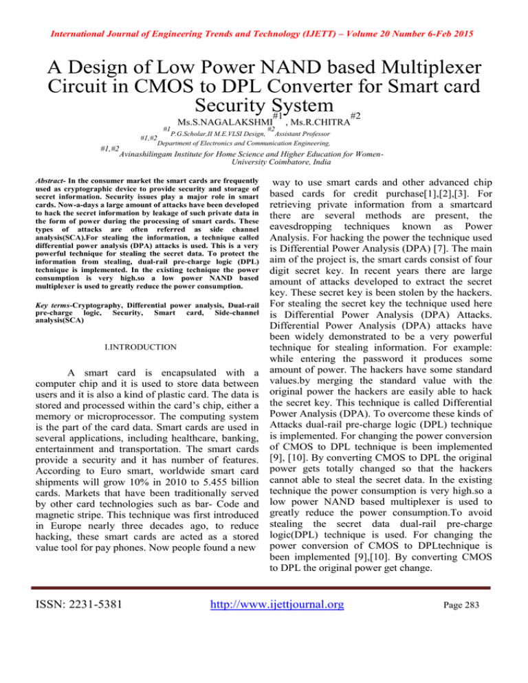
International Journal of Engineering Trends and Technology (IJETT) – Volume 20 Number 6-Feb 2015 A Design of Low Power NAND based Multiplexer Circuit in CMOS to DPL Converter for Smart card Security System #1 #2 #1 #1,#2 Ms.S.NAGALAKSHMI #2 , Ms.R.CHITRA P.G.Scholar,II M.E.VLSI Design, Assistant Professor #1,#2 Department of Electronics and Communication Engineering, Avinashilingam Institute for Home Science and Higher Education for WomenUniversity Coimbatore, India Abstract- In the consumer market the smart cards are frequently used as cryptographic device to provide security and storage of secret information. Security issues play a major role in smart cards. Now-a-days a large amount of attacks have been developed to hack the secret information by leakage of such private data in the form of power during the processing of smart cards. These types of attacks are often referred as side channel analysis(SCA).For stealing the information, a technique called differential power analysis (DPA) attacks is used. This is a very powerful technique for stealing the secret data. To protect the information from stealing, dual-rail pre-charge logic (DPL) technique is implemented. In the existing technique the power consumption is very high.so a low power NAND based multiplexer is used to greatly reduce the power consumption. Key terms-Cryptography, Differential power analysis, Dual-rail pre-charge logic, Security, Smart card, Side-channel analysis(SCA) I.INTRODUCTION A smart card is encapsulated with a computer chip and it is used to store data between users and it is also a kind of plastic card. The data is stored and processed within the card’s chip, either a memory or microprocessor. The computing system is the part of the card data. Smart cards are used in several applications, including healthcare, banking, entertainment and transportation. The smart cards provide a security and it has number of features. According to Euro smart, worldwide smart card shipments will grow 10% in 2010 to 5.455 billion cards. Markets that have been traditionally served by other card technologies such as bar- Code and magnetic stripe. This technique was first introduced in Europe nearly three decades ago, to reduce hacking, these smart cards are acted as a stored value tool for pay phones. Now people found a new ISSN: 2231-5381 way to use smart cards and other advanced chip based cards for credit purchase[1],[2],[3]. For retrieving private information from a smartcard there are several methods are present, the eavesdropping techniques known as Power Analysis. For hacking the power the technique used is Differential Power Analysis (DPA) [7]. The main aim of the project is, the smart cards consist of four digit secret key. In recent years there are large amount of attacks developed to extract the secret key. These secret key is been stolen by the hackers. For stealing the secret key the technique used here is Differential Power Analysis (DPA) Attacks. Differential Power Analysis (DPA) attacks have been widely demonstrated to be a very powerful technique for stealing information. For example: while entering the password it produces some amount of power. The hackers have some standard values.by merging the standard value with the original power the hackers are easily able to hack the secret key. This technique is called Differential Power Analysis (DPA). To overcome these kinds of Attacks dual-rail pre-charge logic (DPL) technique is implemented. For changing the power conversion of CMOS to DPL technique is been implemented [9], [10]. By converting CMOS to DPL the original power gets totally changed so that the hackers cannot able to steal the secret data. In the existing technique the power consumption is very high.so a low power NAND based multiplexer is used to greatly reduce the power consumption.To avoid stealing the secret data dual-rail pre-charge logic(DPL) technique is used. For changing the power conversion of CMOS to DPLtechnique is been implemented [9],[10]. By converting CMOS to DPL the original power get change. http://www.ijettjournal.org Page 283 International Journal of Engineering Trends and Technology (IJETT) – Volume 20 Number 6-Feb 2015 II.TYPES OF ATTACKS A.LPA Attacks A leakage power analysis (LPA) attack is of analyzing the leakage power and hacking the secret key[11]. The hacking is done by tracing out the password of the user[12]. B.DPA Attacks Whenever a user inserts a smartcard into a machine the pin identification number will be recognized. Each and every number in the pin of the smart card will have some leakage power.The hackers who are interested of stealing the secret information(pin number) will merge the leakage power with their corresponding standard box values and will trace the exact pin of the user. Such an attack is called Differential power analysis (DPA) attacks[13]. Dual-rail pre-charge logic (DPL) is an efficient technique. By using DPL technique we can avoid stealing of the secret data. To avoid stealing of the secret data some process of converting CMOS to DPL is being done[14],[15]. DPLs were specifically implemented with the aim of decorrelating the dependence of the dynamic power consumption on the logic data transitions by balancing the energy for each clock cycles and data input[16]. III.LEAKAGE CURRENT IN COMBINATORIAL GATES A.Standard CMOS Logic Fig 1.Data path of the crypto core designed for mounting LPA The fig 2 represents the block diagram. Here input and password is given for the process. When we are swiping the ATM card it has some identification key to recognize that is represented as an input and the password is represented as key.Once when it entered in to Conversion of CMOS to DPL it is been entered as binary value.By converting CMOS to DPL the power is being changed when compare to original power. So that the hackers cannot able to stole the secret key. In Fig 1, the leakage current has been measured on VDD pin of the input converters and the internal DRP logic. Each NMOS and PMOS transistor of a CMOS cell exhibits a static power consumption which contributes to the total leakage of the cell itself. The concept of CMOS to DPL is when clock=1 the output will be Y=1 and Y bar=1.when clock=0 the output will be the inversion of mux output either 10 or 01. B. Dual-Rail pre-charge logic ISSN: 2231-5381 attacks Fig 2: Circuit for the conversion of a CMOS signal into the DPL domain The user’s pin number is given as the input to one of the CMOS to DPL converter and the password is given as key to another block of CMOS to DPLconverter[17].After the input and the key values entered into the conversion of CMOS to DPL block the process takes places.After the process complete the binary value will be stored in register 4 bit. The output of register 4 bit value is been done a XOR operation and send to 4 bit s-box. http://www.ijettjournal.org Page 284 International Journal of Engineering Trends and Technology (IJETT) – Volume 20 Number 6-Feb 2015 The s-box is defined as substitution box for the original value there is a substitution value. That substitution value substitution box.For Example: The original value is 2 for that original value we should refer the Substitution box. So instead of 2 we have some will be stored in register 4 bit and finally the other value like 8,4etc. So that value will be conversionof DPL to CMOS will takes places.So replaced for the original value.This is called as the final output will be the inverse of 4 bit s- Substitution box. box[18]. Fig 4: Substitution Box Fig 3: Existing Technique This is the example of Existing Technique where the 4 digit input is given for process. Only single digit is been under process because here we are using register 4 bit. In existing technique by using differential power analysis(DPA) there is an enriched possibility for hacking the secret information[19]. But when we are converting to CMOS to DPL the exact power of the original data will be totally changed so that the hackers cannot able to steal the original data. for example the exact power of the original data is 3mv.when we are converting to CMOS to DPL the exact power will be change to 6mv.so that the hackers cannot able to steal the original data[20]. IV. ARCHITECTURE OF SUBSTITUTION-BOX In cryptography, an S-box (substitution box) is a Basic component of symmetric key algorithms which performs substitution[21].S-box is a substitution box for the original value we have some standard value takes some number of input bits is represented as m,and transforms them in some number of output bits is represented as n, where n is not Equivalent to m. this is called as ISSN: 2231-5381 S1 S2 Fig 5: Substitution Box For example, each and every value in substitution box S1 will have corresponding equivalent value in Substitution box S2.these values are in turn stored in register of 4 bit. V. LPA ATTACK AGAINST DPL When the clock is stopped during a leakage measurement the output of the CMOS-DPL converters at the interface of the DPL crypto-core, which should convert the signals according to a time difference between the dual-rail pair, are forced to be in an invalid logic state (1,1). In the circuit architecture of the converter is depicted [10].When clock is maintained in a certain logic state, the output lines are forced to be always at the same values. http://www.ijettjournal.org Page 285 International Journal of Engineering Trends and Technology (IJETT) – Volume 20 Number 6-Feb 2015 The operation of CMOS to DPL domain is of when clock=1both the transistor will be active so Y=1 and Y bar =1.and when clock= 0 the output will be the inversion of the mux output either 10 or 01.the output does no more depend on the information to be encoded[22]. VI. PROPOSED WORK automatically the power will get reduce.so finally the power get reduced when compared to the existing technique.in the existing technique the power is 65.but in the proposed technique the power is reduced to 60.The low power NAND based multiplexer is used to reduce the power VII. SIMULATION RESULTS Fig 7:Simulation results of CMOS to DPL conversion Fig 6:Low power NAND based multiplexer The component used in proposed work is NAND gate and the inverter. The use of NAND gate is that NAND gate is a popular logic element because it can be used as a universal gate. The logic NAND gate is a combination of the digital logic and gate with that of an inverter or not gate connected together in series. The NAND gate has an output that is normally at logic level “1” and only goes Fig 8: Power report of CMOS to DPL Technique “low” to logic level “0” when all of its inputs are at logic level “1”.the logic NAND gate is the reverse or complementary form of the AND gate we have seen previously. The use of inverter is that it inverts the input and produces the output. The use of low power NAND based multiplexer is to reduce the power compared to the existing technique. In the existing technique we have used a normal multiplexer.in the normal multiplexer there is a need of 20transistors.But in the low powerNAND based multiplexer we need only 14 transistor.so the transistor count get decreases in the proposed technique. When transistor count decreases Fig 9:Simulation Results of Low Power NAND based multiplexer ISSN: 2231-5381 http://www.ijettjournal.org Page 286 International Journal of Engineering Trends and Technology (IJETT) – Volume 20 Number 6-Feb 2015 [11] L. Lin and W. P. Burleson, “Analysis and mitigation of process variationimpacts on Power-Attack Tolerance,” in Proc. Design AutomationConf. (DAC), 2009, pp. 238–243. [12] Int. Tech. Roadmap for Semiconductors. (2008) [Online].Available:http://public,itrs.net [13] A. Abdollahi, F. Fallah, andM. Pedram, “Leakage current reduction inCMOS VLSI circuits by input vector control,” IEEE Trans. Very LargeScaleIntegr. (VLSI) Syst., vol. 12, no. 2, pp. 140–154, 2004. [14] L. Lin and W. Burleson, “Leakage-based differential power analysis (LDPA) on sub-90nm CMOS cryptosystems,” in Proc. IEEE Int. Symp.Circuits Syst. (ISCAS), 2008, pp. 252–255. [15] H. Saputra, N. Vijaykrishnan, M. Kandemir, M. J. Irwin, R. Brooks,S. Kim, and W. Zhang, “Masking the energy behavior of des encryption,”inProc. IEEE Design, Automation Test Europe Conf. Exhibition—DATE, 2003, pp. 84– 89. [16] M. Alioto, M. Poli, and S. Rocchi, “A general powermodel of differentialpower analysis attacks to static logic circuits,”IEEE Trans. VeryLarge Scale Integr. (VLSI) Syst., vol. 18, no. 5, pp. 711–724,May 2010. Fig 10: Power report of Low Power NAND based multiplexer [17] M. Alioto,M. Poli, and S. Rocchi, “Differential powerAnalysisattackstoprecharged busses: a General analysis for symmetricVIII. CONCLUSION key cryptographic algorithms,” IEEE Trans. Dependable Secure Comput., vol. 7, no. 3, pp. 226–239, Sep. 2010. [18]J. Giorgetti, G. Scotti, A. Simonetti, and A. Trifiletti, “Analysis of By using the differential power analysis Datadependence of leakage current in CMOS cryptographic hardware,” in (DPA) the secret data is been stolen by the hackers. Proc.Great Lake Symp. VLSI (GSLVLSI 2007), Stresa, Italy, Mar. 11,2007, This attack is reduced by using the technique [19] L. Giancane, M. Jovanovich, G. Scotti, and A. Trifiletti,“Leakagepower analysisofcryptographicdevicesimplementedInnanometerCMOS called dual-rail pre-charge logic(DPL).The Low technologies,” in Proc. Konferencija9-a 07: KonferencijazElektroniku, Telekomunikacije, Racunarstvo, Automatiku i NuklearnuTehniku, Herceg Novi Power NAND gate based multiplexer is proposed (Montenegro), Jun. 2007, pp. 355–367. to overcome the power drawbacks in CMOS to [20] M. Alioto, L. Giancane, G. Scotti, and A. Trifiletti, “Leakage poweranalysis attacks: Well-defined procedure and first experimental DPL block in the LPA Attack architecture. results,”inProc. Int. Conf. Microelectron. (ICM), 2009, pp. 46–49. [21] M. Alioto, L. Giancane, G. Scotti, and A. Trifiletti, “Leakage poweranalysis attacks: A Novel class of attacks to nanometer cryptographic circuits,” IEEE Trans. Circuits Syst. I, Reg. Papers, vol. 57, no. 2, pp.355–367, Feb. 2010. [22] M. Djukanovic, L. Giancane, G. Scotti, and A. Trifiletti, “Impact of process variations on LPA attacks effectiveness,” in Proc. Int. Conf. Computer Elect. Eng. (ICCEE09), 2009, pp. 102–106 REFERENCE [1] T. S. Messerges, E. A. Dabbish, and R. H. Sloan, “Examining smartcard security under the threat of power analysis attacks,” IEEE Trans.Comput., vol. 51, no. 5, pp. 541–552, 2002. [2] S. Mangard, E. Oswald, and T. Popp, Power Analysis Attacks: Revealing the Secrets of Smart Cards. New York, NY, USA: Springer-Verlag, 2007. [3] K. Tiri and I. Verbauwhede, “Simulation models for side-channel information leaks,” in Proc. 42ndDesign Automation Conference (DAC), 2005, pp. 228–233. [4] P. C. Kocher, J. Jaffe, and B. Jun, “Differential power analysis,” Proc. CRYPTO’99, pp. 388–397, 1999.ALIOTO et al.: EFFECTIVENESS OF LEAKAGE POWER ANALYSIS ATTACKS 441 [5] K. Tiri and I. Verbauwhede, “A logic level design methodology for a secureDPAresistant ASIC or FPGA implementation,” in Proc.Design,Automation Test Eur. Conf. Expo. (DATE ’04), 2004, pp. 246– 251. [6] K. Tiri and I. Verbauwhede, “A digital design flow for secure integratedcircuits,” IEEE Trans. Computer-Aided Design Integr.CircuitsSyst.,vol. 25, no. 7, pp. 1197–1208, 2006. [7] T. Popp and S. Mangard, “Masked Dual-Rail Pre-charge logic: DPAresistance without routing constraints ,” in Proc. CHES’05, Scotland,UK, Sep. 2005, vol. 3659, pp. 172–186. [8] K. Tiri, M. Akmal, and I. Verbauwhede, “A dynamic and differentialCMOS logic with signal independent power consumption to withstanddifferential power analysis on smart cards,” in Proc. ESSCIRC02, 2002, pp. 403–406. [9] M. Bucci, L. Giancane, R. Luzzi, and A. Trifiletti, “Three-Phase Dual-Rail Pre-Charge logic,” in Proc. Cryptographic Hardware and EmbeddedSyst.— CHES 2006, 8th Int. Workshop, Lecture Notes in ComputerSci. Springer, Yokohama, Japan, Oct. 10–13, 2006. [10] M. Bucci, L. Giancane, R. Luzzi, G. Scotti, and A. Trifiletti, “DelayBased Dual-Rail precharge logic,” IEEE Trans. Very Large Scale Integr.(VLSI) Syst., vol. 19, no. 7, pp. 1147–1153, 2011. ISSN: 2231-5381 http://www.ijettjournal.org Page 287

