Evaluation Board for AD9513/AD9514/
AD9515 Clock Distribution ICs
AD9513/PCB, AD9514/PCB, AD9515/PCB
be set to either LVDS or CMOS. The AD9515 offers two
independent clock outputs, one as LVPECL, the other is
selectable as either LVDS or CMOS levels.
EVALUATION BOARD DESCRIPTION
This data sheet describes the evaluation board for the AD9513,
AD9514, and AD9515 clock distribution ICs.
The LVPECL outputs operate to 1.6 GHz, the LVDS outputs
operate to 800 MHz, and the CMOS outputs operate to 250 MHz.
To properly use the evaluation board, please also reference
the current data sheet for the appropriate part. The current
data sheet is available on the Analog Devices’ website located at
www.analog.com/clocks.
Each output has a programmable divider, which can be set to
divide by a selected set of integers ranging from 1 to 32. The
phase of one clock output relative to another clock output is set
by means of a divider phase select function that serves as a
coarse timing adjustment.
DEVICE DESCRIPTION
The AD9513, AD9514, and AD9515 clock ICs provide multioutput clock distribution in a design that emphasizes low jitter
and phase noise to maximize data converter performance.
Other applications with demanding phase noise and jitter
requirements also benefit from these parts.
The LVDS/CMOS outputs feature a delay element with three
selectable full-scale delay values (1.8 ns, 6.0 ns, and 11.6 ns),
each with 16 steps of fine adjustment.
The AD9513/AD9514/AD9515 clock ICs do not require an
external controller for operation or setup. These devices are
programmed by means of 11 pins (S0 to S10) using 4-level logic.
The required logic levels are provided by the parts.
The AD9513 offers three independent clock outputs, selectable
as either LVDS or CMOS levels. The AD9514 provides three
outputs, two of which are LVPECL outputs, while the third can
05631-001
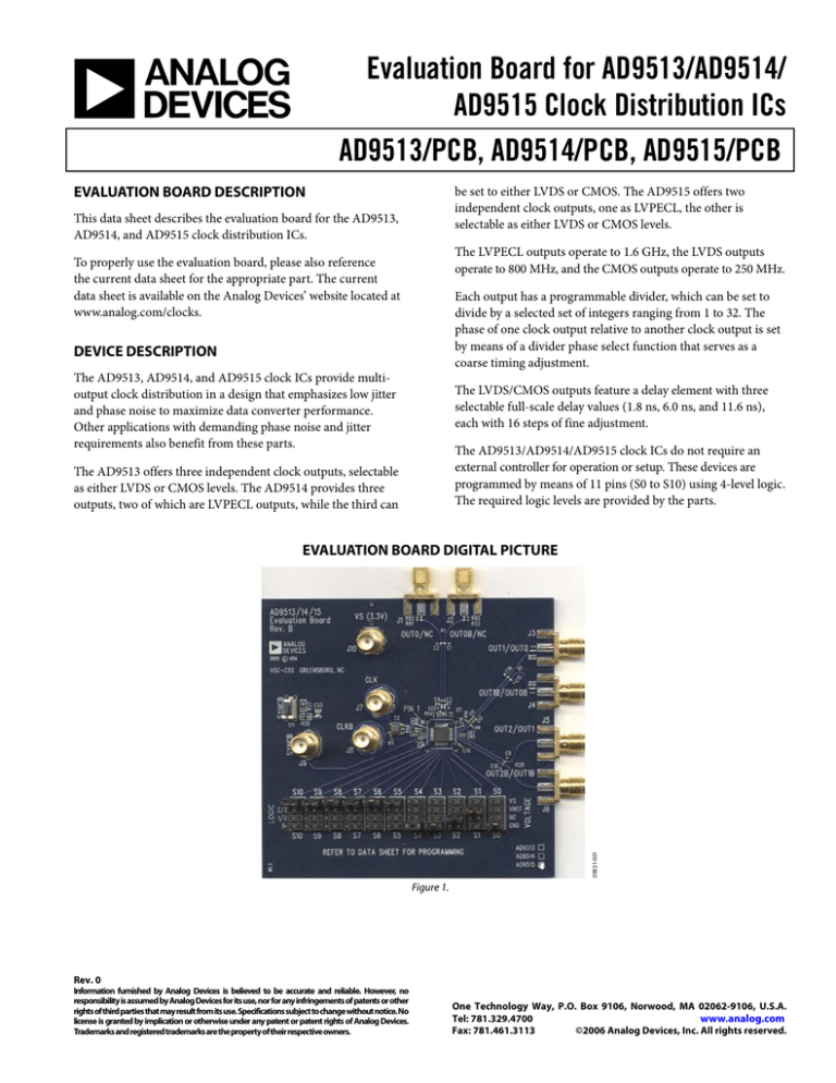
EVALUATION BOARD DIGITAL PICTURE
Figure 1.
Rev. 0
Information furnished by Analog Devices is believed to be accurate and reliable. However, no
responsibility is assumed by Analog Devices for its use, nor for any infringements of patents or other
rights of third parties that may result from its use. Specifications subject to change without notice. No
license is granted by implication or otherwise under any patent or patent rights of Analog Devices.
Trademarks and registered trademarks are the property of their respective owners.
One Technology Way, P.O. Box 9106, Norwood, MA 02062-9106, U.S.A.
Tel: 781.329.4700
www.analog.com
Fax: 781.461.3113
©2006 Analog Devices, Inc. All rights reserved.
AD9513/PCB, AD9514/PCB, AD9515/PCB
TABLE OF CONTENTS
Evaluation Board Description......................................................... 1
Configuring the Board......................................................................4
Device Description........................................................................... 1
Inputs ..............................................................................................4
Evaluation Board Digital Picture.................................................... 1
Outputs ...........................................................................................4
Revision History ............................................................................... 2
Schematics ..........................................................................................5
Setting up the Evaluation Board..................................................... 3
Ordering Information.......................................................................7
Hardware ....................................................................................... 3
Ordering Guide .............................................................................7
Software ......................................................................................... 3
ESD Caution...................................................................................7
Programming the Board.............................................................. 3
REVISION HISTORY
2/06—Revision 0: Initial Version
Rev. 0 | Page 2 of 8
AD9513/PCB, AD9514/PCB, AD9515/PCB
SETTING UP THE EVALUATION BOARD
HARDWARE
The AD9513/AD9514/AD9515 evaluation board requires a 3.3 V
power supply. Some form of input clock must be provided,
usually from a signal generator. A high speed oscilloscope is
helpful in order to see the waveforms present at the clock outputs.
SOFTWARE
No software is required to program the
AD9513/AD9514/AD9515. All of the programming of the part
is provided by the headers and shunts on the evaluation board
itself (see the Programming the Board section).
PROGRAMMING THE BOARD
The digital logic on the AD9513/AD9514/AD9515 is
completely combinational and controlled by the 11 pins labeled
S0 to S10. Each of these pins must be set to one of four voltage
levels (four-state logic). A set of four-position headers is
provided to allow for programming the part using removable
shunts.
Four-State Digital Logic
Table 1 shows the four-state digital logic inputs and their logic
levels and voltages.
Table 1. Four-State Digital Logic Voltage Settings
Logic
1
⅔
Input
VS
VREF
Voltage
3.3 V
⅔ (VS)
⅓
N/C
⅓ (VS)
0
GND
0V
Description
Tie pin to VS.
Internally generated voltage
reference provided at Pin VREF.
Can drive up to all of the logic inputs.
Do not use for other purposes.
Internal self-bias of pin. Leave pin as
no connect.
Tie pin to ground.
The ⅔ (VS) voltage is set by connecting the input to the VREF
pin on the chip. The ⅓ (VS) voltage is obtained by not driving
the input pin at all, thus allowing it to self-bias.
To program the AD9513/AD9514/AD9515 evaluation board,
first determine the logic levels/voltages that should be applied
to the digital inputs. A programming reference appears in the
data sheet. Set each of the programming pins (S0 to S10) to the
appropriate logic level by attaching a shunt to the proper
position on each of the four-position headers.
To the left of the row of headers, a label indicates the logic level
of each row of pins. To the right of the row of headers, a
corresponding label indicates the voltage level of each row of
pins. Note that the row corresponding to a logic level of ⅓
shows that the connection is N/C. When the ⅓ logic level is
needed, the shunt should be placed on the pins, but there is no
connection to the device pin for this logic level.
To program the AD9513 to have all outputs on in LVDS mode,
for example, the S2 and S1 programming pins must be set to
⅓ (VS). On the AD9513/AD9514/AD9515 evaluation board,
locate the 4-position headers that correspond to digital inputs
S2 and S1. Then, referring to the label to the left side of the row
of headers, attach the shunts across the pins corresponding to
the marking for logic level ⅓. Note that the label to the right of
the row of headers indicates that this is an N/C as far as voltage is
concerned.
Rev. 0 | Page 3 of 8
AD9513/PCB, AD9514/PCB, AD9515/PCB
CONFIGURING THE BOARD
INPUTS
Clock Input
AD9514
The input clock is configured to receive a single-ended signal
from bench hardware and convert it to a differential signal at
the part. This is done by a balun, terminated with a 50 Ω
resistor, followed by coupling capacitors on both the true and
complimentary inputs of the part.
The AD9514 has two LVPECL output and one LVDS/CMOS
outputs. OUT0 and OUT1 are both LVPECL. Each LVPECL
output is terminated with a 200 Ω resistor to ground, followed
by an ac coupling capacitor. There are pads for an alternate
termination scheme on the evaluation board. This alternate
scheme creates a Thevenin equivalent 50 Ω termination to
VS − 2 V. This scheme is utilized by removing the 200 Ω
resistors to ground, replacing the ac coupling cap with a 0 Ω
resistor and adding the appropriate termination resistors. These
resistors attach to the pads located near the SMA connectors.
SYNCB Circuit
The SYNCB input allows a sync pulse to be produced without
requiring external circuitry. The evaluation board is populated
with both a momentary switch and an SMA connector labeled
SYNCB. To create a SYNCB signal, depress the momentary switch.
To release the SYNCB signal, release the momentary switch.
An external SYNCB signal can also be applied to the evaluation
board through a cable connected to the SMA connector labeled
SYNCB.
The LVDS/CMOS output (OUT2) is terminated with a 100 Ω
resistor on the evaluation board with the assumption that LVDS
is selected. To use CMOS outputs, this 100 Ω resistor should be
removed.
AD9515
OUTPUTS
AD9513
The AD9513 has three LVDS/CMOS outputs. These outputs are
all terminated with a 100 Ω resistor on the evaluation board
with the assumption that LVDS is selected. To use CMOS
outputs, this 100 Ω resistor should be removed.
The AD9515 has the same default termination scheme and
options as the AD9514. The only difference is that the AD9515
has only one LVPECL output, and one LVDS/CMOS output.
Rev. 0 | Page 4 of 8
05631-002
GND
1
3
4
T2
5
J1
1
Rev. 0 | Page 5 of 8
S11
C43
C46
2
_F
1NF
C33
8
7
6
5
4
3
2
1
U1
31
10
32
9
VREF
29
12
30
11
C2
C4
28
C34
13
J2
27
14
C3
26
15
_F
25
16
C1
GND
17
18
19
20
21
22
23
24
C9
Figure 2. AD9513/AD9514/AD9515 Evaluation Board Schematic, Page 1
_F
C10
_F
C13
C11
C16
_F
C15
_F
J6
J5
J4
J3
C67
C23
C65
C27
C70
C28
C5
C31
C6
VS
C14
AD9513/PCB, AD9514/PCB, AD9515/PCB
SCHEMATICS
VS
Rev. 0 | Page 6 of 8
Figure 3. AD9513/AD9514/AD9515 Evaluation Board Schematic, Page 2
05631-003
GND
VREF
VS
GND
VREF
VS
GND
VREF
4
6
8
2
4
6
8
5
7
1
3
5
7
8
7
2
6
5
3
4
3
1
2
1
S10
S5
S0
VS
GND
VREF
VS
GND
VREF
7
5
3
1
7
5
3
1
8
6
4
2
8
6
4
2
S6
S1
VS
GND
VREF
VS
GND
VREF
7
5
3
1
7
5
3
1
8
6
4
2
8
6
4
2
S7
S2
VS
GND
VREF
VS
GND
VREF
7
5
3
1
7
5
3
1
8
6
4
2
8
6
4
2
S8
S3
VS
GND
VREF
VS
GND
VREF
7
5
3
1
7
5
3
1
8
6
4
2
8
6
4
2
S9
S4
AD9513/PCB, AD9514/PCB, AD9515/PCB
AD9513/PCB, AD9514/PCB, AD9515/PCB
ORDERING INFORMATION
ORDERING GUIDE
Model
AD9513/PCB
AD9514/PCB
AD9515/PCB
Description
Evaluation Board
Evaluation Board
Evaluation Board
ESD CAUTION
ESD (electrostatic discharge) sensitive device. Electrostatic charges as high as 4000 V readily accumulate on
the human body and test equipment and can discharge without detection. Although this product features
proprietary ESD protection circuitry, permanent damage may occur on devices subjected to high energy
electrostatic discharges. Therefore, proper ESD precautions are recommended to avoid performance
degradation or loss of functionality.
Rev. 0 | Page 7 of 8
AD9513/PCB, AD9514/PCB, AD9515/PCB
NOTES
©2006 Analog Devices, Inc. All rights reserved. Trademarks and
registered trademarks are the property of their respective owners.
EB05631-0-2/06(0)
Rev. 0 | Page 8 of 8


