3.1 CERAMICS AS ELECTRICAL CONDUCTORS
advertisement
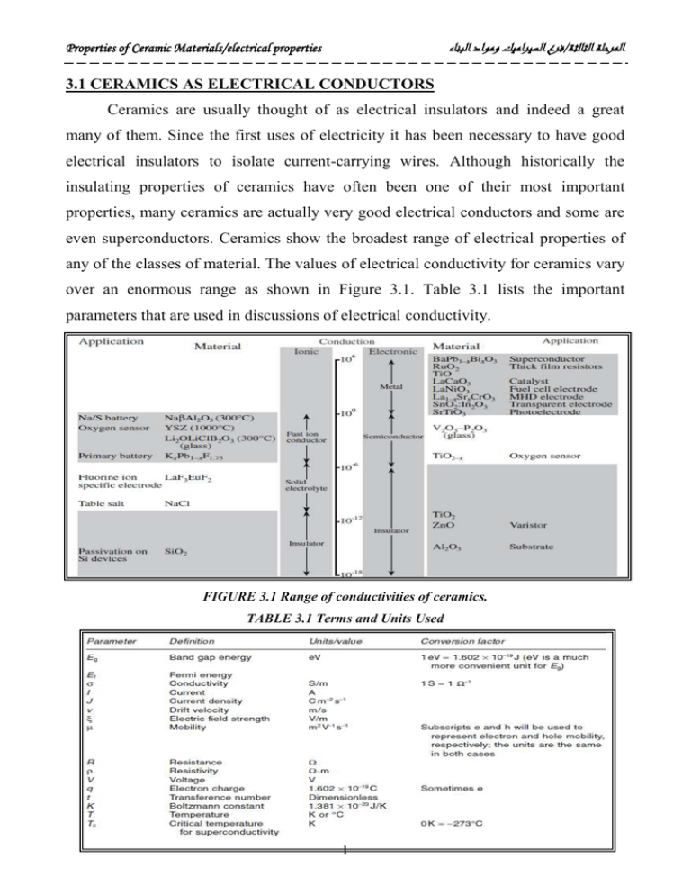
فرع السيراميك ومواد البناء/المرحلة الثالثة Properties of Ceramic Materials/electrical properties 3.1 CERAMICS AS ELECTRICAL CONDUCTORS Ceramics are usually thought of as electrical insulators and indeed a great many of them. Since the first uses of electricity it has been necessary to have good electrical insulators to isolate current-carrying wires. Although historically the insulating properties of ceramics have often been one of their most important properties, many ceramics are actually very good electrical conductors and some are even superconductors. Ceramics show the broadest range of electrical properties of any of the classes of material. The values of electrical conductivity for ceramics vary over an enormous range as shown in Figure 3.1. Table 3.1 lists the important parameters that are used in discussions of electrical conductivity. FIGURE 3.1 Range of conductivities of ceramics. TABLE 3.1 Terms and Units Used 1 فرع السيراميك ومواد البناء/المرحلة الثالثة Properties of Ceramic Materials/electrical properties Fortunately, the electrical properties of materials can largely be understood by assuming that they are isotropic and σ is simply a scalar. The conduction mechanisms in ceramics can be quite complex and may involve the movement of electrons, holes, and ions; in some cases they may be “mixed,” with more than one type of charge carrier responsible for current flow. In the case of ceramic superconductors the current is carried by electron pairs (Cooper pairs). So this is really very different and is discussed separately. In comparing values of σ and ρ it is useful to remember the simple relationship between them: (3.1) 3.2 CONDUCTION MECHANISMS IN CERAMICS Electrical conductivity is given by (3.2) The importance of Eq. 3.2 is that it applies to all materials and it shows that the two factors affecting σ are - Number of charge carriers, n - Their mobility, μ When we consider the effect of variables such as composition, structure, and temperature on σ we are concerned with their effect on n and μ. If more than one type of charge carrier is contributing to σ then we can define a partial conductivity for each. For example, if σ were due to the movement of electrons and cations with a charge Z, then for electrons (3.3) and for cations (3.4) The total is (3.5) If a ceramic is an electron conductor, i.e., te =1, then to determine n we need to know Eg. We usually consider the three situations shown in Figure 3.2, where the band gap is either zero, narrow, or wide. 2 فرع السيراميك ومواد البناء/المرحلة الثالثة Properties of Ceramic Materials/electrical properties FIGURE 3.2 Schematic of electron energy bands in solids. The valence band (VB) and conduction band (CB) are indicated. The real band structure of a material is actually a complex three-dimensional shape. Even so these simple representations can be used to illustrate many of the important electronic properties of materials. When Eg is zero, as in the case of most metals, there are free electrons present at any temperature above 0 K. The total number of free electrons is equal to the number of valence electrons per atom multiplied by the number of atoms in the metal. Eg in a metal is not zero, but it is very small. For example, if we have a metal crystal consisting of 1023 atoms and the width of the energy band is 1 eV then the separation between the energy levels would be only 10−23 eV (1.6 *10−42 J). This would be the minimum amount of energy required to excite an electron into a vacant level. A narrow band gap is usually defined as being in the range of 0.02 to about 2.5 eV. When Eg is toward the lowest end of this range there is a significant fraction of electrons in the conduction band. Materials with a narrow band gap are usually referred to as semiconductors. - Silicon: Eg =1.12 eV - Gallium arsenide: Eg =1.42 eV (Both Si and GaAs are ceramics). Materials with a wide band gap (>2.5 eV) are considered to be electrical insulators because the probability of an electron being in the conduction band at room temperature is extremely small. However, the probability is not zero and so we should think of these materials as wideband- gap semiconductors. SiC (Eg =2.6–3.0) is an example of a wide-band-gap semiconductor and is used in sensors in aircraft 3 فرع السيراميك ومواد البناء/المرحلة الثالثة Properties of Ceramic Materials/electrical properties and fuel cells that can operate in hostile environments at temperatures up to 600°C where conventional silicon-based electronics cannot function. ●TRANSFERENCE NUMBER The transference or transport number is the fraction of σtot contributed by each charge carrier. For electrons: te = σe/σtot For cations: t+=σ+ /σtot 3.3 NUMBER OF CONDUCTION ELECTRONS The number of electrons in the conduction band, ni, is (3.6) - Nc(E) dE is the density of states in the conduction band represents the number of energy levels over which the electrons can be distributed (i.e., the number of allowed energy states). - P (E) is the Fermi–Dirac function giving the probability of an electron being in the conduction band. (3.7) The evaluation of ni is quite straightforward if we make the following assumptions: 1. E − Ef >>kT. This is often the case since at room temperature kT ~ 0.025 eV and E − Ef is usually >5 eV. 2. The excited electrons occupy states near the bottom of the conduction band. Under these conditions they behave as free particles for which the state distribution function is known. 3. The upper limit of the integration in Eq. 3.6 is taken as ∞since the probability of occupancy of a state by an electron rapidly approaches zero as the energy increases through the band. Under these assumptions we can write (3.8) 4 فرع السيراميك ومواد البناء/المرحلة الثالثة Properties of Ceramic Materials/electrical properties EF lies midway between EC and EV in an intrinsic material (i.e., one that has few impurities) and since NC ~1025 m−3 we can simplify Eq. 3.8 as (3.9) The important things to remember from this series of equations are that - n depends on Eg and T. - As we increase T we increase n. 5
