Document 12534726
advertisement
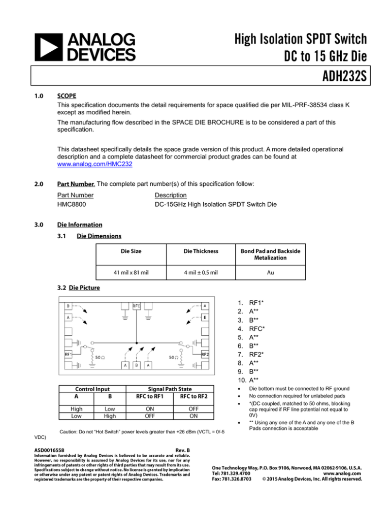
This specification documents the detail requirements for space qualified die per MIL-PRF-38534 class K except as modified herein. The manufacturing flow described in the SPACE DIE BROCHURE is to be considered a part of this specification. This datasheet specifically details the space grade version of this product. A more detailed operational description and a complete datasheet for commercial product grades can be found at www.analog.com/HMC232 The complete part number(s) of this specification follow: Part Number HMC8800 Description DC-15GHz High Isolation SPDT Switch Die 1. 2. 3. 4. 5. 6. 7. 8. 9. 10. RF1* A** B** RFC* A** B** RF2* A** B** A** Die bottom must be connected to RF ground No connection required for unlabeled pads *(DC coupled, matched to 50 ohms, blocking cap required if RF line potential not equal to 0V) ** Using any one of the A and any one of the B Pads connection is acceptable Caution: Do not “Hot Switch” power levels greater than +26 dBm (VCTL = 0/-5 VDC) RF Input Power (Vctl = -5V) (0.5 – 15GHz) ................ +30dBm (@ +50⁰C) Control Voltage Range (A & B) ......................................... +1 V to -7.5 Vdc Channel Temperature ....................................................................... 150C Thermal resistance .........................................................................92C/W Storage Temperature ........................................................-65C to +150C Operating Temperature .......................................................-40C to +80C ESD Sensitivity (HBM) .................................................................. Class 1A Absolute Maximum Ratings Notes: 1/ Stresses above the absolute maximum rating may cause permanent damage to the device. Extended operation at the maximum levels may degrade performance and affect reliability. In accordance with class-K version of MIL-PRF-38534, Appendix C, Table C-II, except as modified herein. (a) Qual Sample Size and Qual Acceptance Criteria – 10/0 (b) Pre-screen test post assembly required prior to die qualification, to remove all assembly related rejects. (c) Mechanical Shock or Constant Acceleration not performed; die qualification is performed in an open carrier . (d) Max die qualification temperature limited to +85C Table I Notes: 1. 2. 3. 4. Limits apply at +25C only. Tested with VCTLA/B Low = -0.2V, High = -5V S-par data to be tabulated at 50MHz and every 1GHz, 1GHz to 15GHz. Pin = -25dBm P1dB shall be measured at 5GHz, 10GHz, 15GHz, Go-No-Go Table II Notes: 1/ 2/ 3/ 4/ 5/ 6/ Pre burn-in and Post burn-in electrical require S-parameter testing only as defined. Final electrical tests shall incorporate power tests as defined. Temperature testing required for Final Electrical testing only Tested with VCTLA/B Low = -0.2 V, High = -5 V S-par data to be tabulated at 50MHz and every 1 GHz, 1 GHz to 15 GHz. Pin = -25 dBm P1dB shall be measured at 1 GHz to 17 GHz, 2 GHz steps IP3 shall be measured at 1 GHz to 17GHz, 2 GHz steps Table III Notes: 1/ Table II limits will not be exceeded 2/ 240 hour burn in and Group C end point electrical parameters. Deltas are performed at TA = 25°C 11. 12. 13. 14. 15. 16. 17. 18. 19. 20. RF1* A** B** RFC* A** B** RF2* A** B** A** Die bottom must be connected to RF ground No connection required for unlabeled pads *(DC coupled, matched to 50 ohms, blocking cap required if RF line potential not equal to 0V) ** Using any one of the A and any one of the B Pads connection is acceptable
