Small and Thin ±2 g Accelerometer
ADXL322
FEATURES
GENERAL DESCRIPTION
Small and thin
4 mm × 4 mm × 1.45 mm LFCSP package
2 mg resolution at 60 Hz
Wide supply voltage range: 2.4 V to 6 V
Low power: 340 μA at VS = 2.4 V (typ)
Good zero g bias stability
Good sensitivity accuracy
X-axis and Y-axis aligned to within 0.1° (typ)
BW adjustment with a single capacitor
Single-supply operation
10,000 g shock survival
Pb Free: Compatible with Sn/Pb and Pb-free solder processes
The ADXL322 is a small, thin, low power, complete, dual-axis
accelerometer with signal conditioned voltage outputs, which
are all on a single monolithic IC. The product measures acceleration with a full-scale range of ±2 g (typical). It can also
measure both dynamic acceleration (vibration) and static
acceleration (gravity).
The ADXL322’s typical noise floor is 220 μg/√Hz, which allows
signals below 2 mg to be resolved in tilt-sensing applications
using narrow bandwidths (<60 Hz).
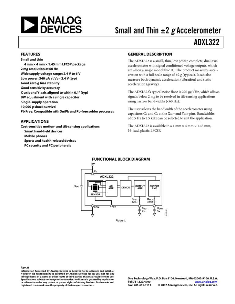
The user selects the bandwidth of the accelerometer using
capacitors CX and CY at the XOUT and YOUT pins. Bandwidths
of 0.5 Hz to 2.5 kHz can be selected to suit the application.
APPLICATIONS
The ADXL322 is available in a 4 mm × 4 mm × 1.45 mm,
16-lead, plastic LFCSP.
Cost-sensitive motion- and tilt-sensing applications
Smart hand-held devices
Mobile phones
Sports and health-related devices
PC security and PC peripherals
FUNCTIONAL BLOCK DIAGRAM
+3V
VS
ADXL322
CDC
AC
AMP
DEMOD
OUTPUT
AMP
OUTPUT
AMP
SENSOR
COM
ST
RFILT
32kΩ
YOUT
CY
XOUT
CX
05589-001
RFILT
32kΩ
Figure 1.
Rev. 0
Information furnished by Analog Devices is believed to be accurate and reliable.
However, no responsibility is assumed by Analog Devices for its use, nor for any
infringements of patents or other rights of third parties that may result from its use.
Specifications subject to change without notice. No license is granted by implication
or otherwise under any patent or patent rights of Analog Devices. Trademarks and
registered trademarks are the property of their respective owners.
One Technology Way, P.O. Box 9106, Norwood, MA 02062-9106, U.S.A.
www.analog.com
Tel: 781.329.4700
Fax: 781.461.3113
© 2007 Analog Devices, Inc. All rights reserved.
ADXL322
TABLE OF CONTENTS
Specifications..................................................................................... 3
Setting the Bandwidth Using CX and CY ................................. 12
Absolute Maximum Ratings............................................................ 4
Self-Test ....................................................................................... 12
ESD Caution.................................................................................. 4
Design Trade-Offs for Selecting Filter Characteristics: The
Noise/BW Trade-Off.................................................................. 12
Pin Configuration and Function Descriptions............................. 5
Typical Performance Characteristics (VS = 3.0 V) ....................... 7
Theory of Operation ...................................................................... 11
Performance ................................................................................ 11
Applications..................................................................................... 12
Use with Operating Voltages Other than 3 V............................. 13
Use as a Dual-Axis Tilt Sensor ................................................. 13
Outline Dimensions ....................................................................... 14
Ordering Guide .......................................................................... 14
Power Supply Decoupling ......................................................... 12
REVISION HISTORY
6/05—Revision 0: Initial Version
Rev. 0 | Page 2 of 16
ADXL322
SPECIFICATIONS
TA = 25°C, VS = 3 V, CX = CY = 0.1 μF, Acceleration = 0 g, unless otherwise noted 1 .
Table 1.
Parameter
SENSOR INPUT
Measurement Range
Nonlinearity
Package Alignment Error
Alignment Error
Cross-Axis Sensitivity
SENSITIVITY (RATIOMETRIC) 2
Sensitivity at XOUT, YOUT
Sensitivity Change due to Temperature 3
ZERO g BIAS LEVEL (RATIOMETRIC)
0 g Voltage at XOUT, YOUT
Initial 0 g Bias Deviation from Ideal
0 g Offset Vs. Temperature
NOISE PERFORMANCE
Noise Density
FREQUENCY RESPONSE 4
CX, CY Range 5
RFILT Tolerance
Sensor Resonant Frequency
SELF-TEST 6
Logic Input Low
Logic Input High
ST Input Resistance to Ground
Output Change at XOUT, YOUT
OUTPUT AMPLIFIER
Output Swing Low
Output Swing High
POWER SUPPLY
Operating Voltage Range
Quiescent Supply Current
Turn-On Time 7
TEMPERATURE
Operating Temperature Range
Conditions
Each axis
Min
Max
X sensor to Y sensor
Unit
g
%
Degrees
Degrees
%
±2
±0.2
±1
±0.1
±2
% of full scale
Each axis
VS = 3 V
VS = 3 V
Each axis
VS = 3 V
Typ
378
420
0.01
462
mV/g
%/°C
1.3
1.5
±50
<±0.5
1.7
V
mg
mg/°C
at 25°C
220
0.002
μg/√Hz rms
32 ± 15%
5.5
10
μF
kΩ
kHz
Self-test 0 to 1
0.6
2.4
50
125
V
V
kΩ
mV
No load
No load
0.2
2.7
V
V
T
2.4
6
V
mA
ms
70
°C
0.45
20
−20
1
All minimum and maximum specifications are guaranteed. Typical specifications are not guaranteed.
Sensitivity is essentially ratiometric to VS. For VS = 2.7 V to 3.3 V, sensitivity is 138 mV/V/g to 142 mV/V/g typical.
3
Defined as the output change from ambient-to-maximum temperature or ambient-to-minimum temperature.
4
Actual frequency response controlled by user-supplied external capacitor (CX, CY).
5
Bandwidth = 1/(2 × π × 32 kΩ × C). For CX, CY = 0.002 μF, bandwidth = 2500 Hz. For CX, CY = 10 μF, bandwidth = 0.5 Hz. Minimum/maximum values are not tested.
6
Self-test response changes cubically with VS.
7
Larger values of CX, CY increase turn-on time. Turn-on time is approximately 160 × CX or CY + 4 ms, where CX, CY are in μF.
2
Rev. 0 | Page 3 of 16
ADXL322
ABSOLUTE MAXIMUM RATINGS
Table 2.
Parameter
Acceleration (Any Axis, Unpowered)
Acceleration (Any Axis, Powered)
VS
All Other Pins
Output Short-Circuit Duration
(Any Pin to Common)
Operating Temperature Range
Storage Temperature
Rating
10,000 g
10,000 g
−0.3 V to +7.0 V
(COM − 0.3 V) to
(VS + 0.3 V)
Stresses above those listed under Absolute Maximum Ratings
may cause permanent damage to the device. This is a stress
rating only; functional operation of the device at these or any
other conditions above those indicated in the operational
section of this specification is not implied. Exposure to absolute
maximum rating conditions for extended periods may affect
device reliability.
Indefinite
−55°C to +125°C
−65°C to +150°C
ESD CAUTION
ESD (electrostatic discharge) sensitive device. Electrostatic charges as high as 4000 V readily accumulate
on the human body and test equipment and can discharge without detection. Although this product features
proprietary ESD protection circuitry, permanent damage may occur on devices subjected to high energy
electrostatic discharges. Therefore, proper ESD precautions are recommended to avoid performance
degradation or loss of functionality.
Rev. 0 | Page 4 of 16
ADXL322
PIN CONFIGURATION AND FUNCTION DESCRIPTIONS
NC
VS
VS
NC
NC
XOUT
ST
ADXL322
NC
COM
TOP VIEW
(Not to Scale)
YOUT
NC
COM COM COM
NC
NC = NO CONNECT
05589-022
NC
Figure 2. Pin Configuration
Table 3. Pin Function Descriptions
Mnemonic
NC
ST
COM
NC
COM
COM
COM
NC
NC
YOUT
NC
XOUT
NC
VS
VS
NC
Description
Do Not Connect
Self-Test
Common
Do Not Connect
Common
Common
Common
Do Not Connect
Do Not Connect
Y-Channel Output
Do Not Connect
X-Channel Output
Do Not Connect
2.4 V to 6 V
2.4 V to 6 V
Do Not Connect
4.000
0.600
MAX
0.325
0.650
0.650
0.350
MAX
1.950
0.325
4.000
1.950
Figure 3. 4 mm × 4 mm 16- pad LFCSP Recommended Pad Layout
Rev. 0 | Page 5 of 16
05589-023
Pin No.
1
2
3
4
5
6
7
8
9
10
11
12
13
14
15
16
ADXL322
CRITICAL ZONE
TL TO TP
tP
TP
TEMPERATURE
RAMP-UP
TL
tL
TSMAX
TSMIN
tS
RAMP-DOWN
05589-002
PREHEAT
t25°C TO PEAK
TIME
Figure 4. Recommended Soldering Profile
Table 4. Recommended Soldering Profile
Profile Feature
Average Ramp Rate (TL to TP)
Preheat
Minimum Temperature (TSMIN)
Minimum Temperature (TSMAX)
Time (TSMIN to TSMAX), tS
TSMAX to TL
Ramp-Up Rate
Time Maintained Above Liquidous (TL)
Liquidous Temperature (TL)
Time (tL)
Peak Temperature (TP)
Time within 5°C of Actual Peak Temperature (tP)
Ramp-Down Rate
Time 25°C to Peak Temperature
Rev. 0 | Page 6 of 16
Sn63/Pb37
3°C/sec max
Pb-Free
3°C/sec max
100°C
150°C
60 sec − 120 sec
150°C
200°C
60 sec − 150 sec
3°C/sec
3°C/sec
183°C
60 sec − 150 sec
240°C + 0°C/−5°C
10 sec − 30 sec
6°C/sec max
6 min max
217°C
60 sec − 150 sec
260°C + 0°C/−5°C
20 sec − 40 sec
6°C/sec max
8 min max
ADXL322
TYPICAL PERFORMANCE CHARACTERISTICS (VS = 3.0 V)
35
40
30
35
30
% OF POPULATION
20
15
10
25
20
15
10
0
05589-007
5
05589-004
5
0
1.40 1.42 1.44 1.46 1.48 1.50 1.52 1.54 1.56 1.58 1.60
1.40 1.42 1.44 1.46 1.48 1.50 1.52 1.54 1.56 1.58 1.60
OUTPUT (V)
OUTPUT (V)
Figure 5. X-Axis Zero g Bias at 25°C
Figure 8. Y-Axis Zero g Bias at 25°C
40
45
35
40
35
% OF POPULATION
25
20
15
10
30
25
20
15
10
05589-005
5
0
–2.0
–1.5
–1.0
–0.5
0
0.5
1.0
1.5
5
0
2.0
–2.0
TEMPERATURE COEFFICIENT (mg/°C)
–1.5
–1.0
–0.5
0
0.5
1.0
1.5
2.0
TEMPERATURE COEFFICIENT (mg/°C)
Figure 6. X-Axis Zero g Bias Temperature Coefficient
Figure 9. Y-Axis Zero g Bias Temperature Coefficient
50
45
45
40
40
35
% OF POPULATION
35
30
25
20
15
30
25
20
15
10
10
5
0
0.400 0.405 0.410 0.415 0.420 0.425 0.430 0.435 0.440 0.445 0.450
05589-006
% OF POPULATION
05589-008
% OF POPULATION
30
5
0
0.400 0.405 0.410 0.415 0.420 0.425 0.430 0.435 0.440 0.445 0.450
SENSITIVITY (V/g)
SENSITIVITY (V/g)
Figure 7. X-Axis Sensitivity at 25°C
Figure 10. Y-Axis Sensitivity at 25°C
Rev. 0 | Page 7 of 16
05589-009
% OF POPULATION
25
0.440
1.575
0.435
1.550
0.430
1.525
1.500
1.475
0.425
0.420
0.415
1.450
0.410
1.425
0.405
1.400
–40
–20
0
20
40
60
0.400
–40
80
05589-013
SENSITIVITY V/g
1.600
05589-010
0g OUTPUT (V)
ADXL322
–20
0
TEMPERATURE (°C)
20
40
60
80
TEMPERATURE (°C)
Figure 11. Zero g Bias vs. Temperature—Parts Soldered to PCB
Figure 14. Sensitivity vs. Temperature—Parts Soldered to PCB
70
45
40
60
35
% OF POPULATION
% OF POPULATION
50
40
30
20
30
25
20
15
05589-012
0
150
160
170
180
190
200
210
220
230
240
05589-015
10
10
5
0
150
250
160
170
180
NOISE μg/ Hz
200
210
220
230
240
250
4
5
NOISE μg/ Hz
Figure 12. X-Axis Noise Density at 25°C
Figure 15. Y-Axis Noise Density at 25°C
25
30
25
% OF POPULATION
20
15
10
5
20
15
10
0
–5
–4
–3
–2
–1
0
1
2
3
4
05589-014
5
05589-011
% OF POPULATION
190
0
–5
5
PERCENT SENSITIVITY (%)
–4
–3
–2
–1
0
1
2
3
PERCENT SENSITIVITY (%)
Figure 13. Z vs. X Cross-Axis Sensitivity
Figure 16. Z vs. Y Cross-Axis Sensitivity
Rev. 0 | Page 8 of 16
25
25
20
20
% OF POPULATION
15
10
10
5
05589-016
5
15
0
0.08
0.09
0.10
0.11
0.12
0.13
0.14
0.15
05589-019
% OF POPULATION
ADXL322
0
0.16
0.08
0.09
0.10
SELF-TEST (V)
0.11
0.12
0.13
0.14
0.15
0.16
SELF-TEST (V)
Figure 17. X-Axis Self-Test Response at 25°C
Figure 19. Y-Axis Self-Test Response at 25°C
60
40
30
20
10
0
370
390
410
430
450
470
490
CURRENT (μA)
Figure 18. Supply Current at 25°C
Figure 20. Turn-On Time—CX, CY = 0.1 μF, Time Scale = 2 ms/DIV
550
500
CURRENT (μA)
450
400
350
300
–40
05589-021
350
05589-020
05589-017
% OF POPULATION
50
–20
0
20
40
60
80
100
TEMPERATURE (°C)
Figure 21. Supply Current vs. Temperature VS=3V
Rev. 0 | Page 9 of 16
120
ADXL322
XL
322J
#1234
5678P
YOUT = 1.50V
XOUT = 1.50V
YOUT = 1.08V
XOUT = 1.92V
YOUT = 1.50V
XOUT = 1.500V
YOUT = 1.500V
EARTH'S SURFACE
Figure 22. Output Response vs. Orientation
Rev. 0 | Page 10 of 16
05589-018
YOUT = 1.92V
XOUT = 1.08V
XL
322J
#1234
5678P
XOUT = 1.50V
XL
322J
#1234
5678P
XL
322J
#1234
5678P
ADXL322
THEORY OF OPERATION
The ADXL322 is a complete acceleration measurement system
on a single monolithic IC. The ADXL322 has a measurement
range of ±2 g. It contains a polysilicon surface micromachined
sensor and signal conditioning circuitry to implement an openloop acceleration measurement architecture. The output signals
are analog voltages that are proportional to acceleration. The
accelerometer measures static acceleration forces, such as
gravity, which allows it to be used as a tilt sensor.
The sensor is a polysilicon surface-micromachined structure
built on top of a silicon wafer. Polysilicon springs suspend the
structure over the surface of the wafer and provide a resistance
against acceleration forces. Deflection of the structure is
measured using a differential capacitor that consists of independent fixed plates and plates attached to the moving mass.
The fixed plates are driven by 180° out-of-phase square waves.
Acceleration deflects the beam and unbalances the differential
capacitor, resulting in an output square wave whose amplitude
is proportional to acceleration. Phase-sensitive demodulation
techniques are then used to rectify the signal and determine
the direction of the acceleration.
PERFORMANCE
Rather than using additional temperature compensation
circuitry, innovative design techniques were used to ensure
built-in high performance. As a result, there is neither quantization error nor nonmonotonic behavior, and temperature
hysteresis is very low (typically less than 5 mg over the −20°C
to +70°C temperature range).
Figure 11 shows the zero g output performance of eight parts
(X- and Y-axis) over a −20°C to +70°C temperature range.
Figure 14 demonstrates the typical sensitivity shift over temperature for supply voltages of 3 V. This is typically better than
±1% over the −20°C to +70°C temperature range.
The demodulator’s output is amplified and brought offchip through a 32 kΩ resistor. The user then sets the signal
bandwidth of the device by adding a capacitor. This filtering
improves measurement resolution and helps prevent aliasing.
Rev. 0 | Page 11 of 16
ADXL322
APPLICATIONS
POWER SUPPLY DECOUPLING
For most applications, a single 0.1 μF capacitor, CDC, adequately
decouples the accelerometer from noise on the power supply.
However, in some cases, particularly where noise is present
at the 140 kHz internal clock frequency (or any harmonic
thereof), noise on the supply can cause interference on the
ADXL322 output. If additional decoupling is needed, a 100 Ω
(or smaller) resistor or ferrite bead can be inserted in the supply
line. Additionally, a larger bulk bypass capacitor (in the 1 μF to
4.7 μF range) can be added in parallel to CDC.
SETTING THE BANDWIDTH USING CX AND CY
The ADXL322 has provisions for band-limiting the XOUT and
YOUT pins. Capacitors must be added at these pins to implement
low-pass filtering for antialiasing and noise reduction. The
equation for the 3 dB bandwidth is
F−3 dB = 1/(2π(32 kΩ) × C(X, Y))
or more simply,
F–3 dB = 5 μF/C(X, Y)
The tolerance of the internal resistor (RFILT) typically varies as
much as ±15% of its nominal value (32 kΩ), and the bandwidth
varies accordingly. A minimum capacitance of 2000 pF for CX
and CY is required in all cases.
DESIGN TRADE-OFFS FOR SELECTING FILTER
CHARACTERISTICS: THE NOISE/BW TRADE-OFF
The accelerometer bandwidth selected ultimately determines
the measurement resolution (smallest detectable acceleration).
Filtering can be used to lower the noise floor, which improves
the resolution of the accelerometer. Resolution is dependent on
the analog filter bandwidth at XOUT and YOUT.
The output of the ADXL322 has a typical bandwidth of 2.5 kHz.
To limit aliasing errors, the user must filter the signal at this
point. The analog bandwidth must be no more than half the
A/D sampling frequency to minimize aliasing. The analog
bandwidth can be further decreased to reduce noise and
improve resolution.
The ADXL322 noise has the characteristics of white Gaussian
noise, which contributes equally at all frequencies and is
described in terms of μg/√Hz (the noise is proportional to the
square root of the accelerometer’s bandwidth). The user should
limit bandwidth to the lowest frequency needed by the application in order to maximize the resolution and dynamic range of
the accelerometer.
With the single-pole, roll-off characteristic, the typical noise of
the ADXL322 is determined by
rmsNoise = (220 μg/ Hz ) × ( BW × 1.6 )
Table 5. Filter Capacitor Selection, CX and CY
Bandwidth (Hz)
1
10
50
100
200
500
At 100 Hz bandwidth the noise will be
Capacitor (μF)
4.7
0.47
0.10
0.05
0.027
0.01
rmsNoise = (220 μg/ Hz ) × ( 100 × 1.6 ) = 2.8 mg
Often, the peak value of the noise is desired. Peak-to-peak noise
can only be estimated by statistical methods. Table 6 is useful
for estimating the probabilities of exceeding various peak
values, given the rms value.
Table 6. Estimation of Peak-to-Peak Noise
SELF-TEST
The ST pin controls the self-test feature. When this pin is set to
VS, an electrostatic force is exerted on the accelerometer beam.
The resulting movement of the beam allows the user to test if
the accelerometer is functional. The typical change in output is
300 mg (corresponding to 125 mV). This pin can be left opencircuit or connected to common (COM) in normal use.
Peak-to-Peak Value
2 × rms
4 × rms
6 × rms
8 × rms
The ST pin should never be exposed to voltages greater than
VS + 0.3 V. If this cannot be guaranteed due to the system
design (for instance, if there are multiple supply voltages), then
a low VF clamping diode between ST and VS is recommended.
Rev. 0 | Page 12 of 16
% of Time That Noise Exceeds
Nominal Peak-to-Peak Value
32
4.6
0.27
0.006
ADXL322
Peak-to-peak noise values give the best estimate of the uncertainty in a single measurement. Table 7 gives the typical noise
output of the ADXL322 for various CX and CY values.
Table 7. Filter Capacitor Selection (CX, CY)
Bandwidth
(Hz)
10
50
100
500
CX, CY
(μF)
0.47
0.1
0.047
0.01
RMS Noise
(mg)
0.9
2
2.8
6.2
Peak-to-Peak Noise
Estimate (mg)
5.3
11.8
16.7
37.3
USE WITH OPERATING VOLTAGES OTHER THAN 3 V
The ADXL322 is tested and specified at VS = 3 V; however, this
part can be powered with VS as low as 2.4 V or as high as 6 V.
Note that some performance parameters change as the supply
voltage is varied.
The ADXL322 output is ratiometric, so the output sensitivity
(or scale factor) varies proportionally to supply voltage. At VS =
5 V, the output sensitivity is typically 750 mV/g. At VS = 2.4 V,
the output sensitivity is typically 335 mV/g.
The zero g bias output is also ratiometric, so the zero g output is
nominally equal to VS/2 at all supply voltages.
The output noise is not ratiometric but is absolute in volts;
therefore, the noise density decreases as the supply voltage
increases. This is because the scale factor (mV/g) increases
while the noise voltage remains constant. At VS = 5 V, the
noise density is typically 150 μg/√Hz, while at VS = 2.4 V,
the noise density is typically 300 μg/√Hz,
USE AS A DUAL-AXIS TILT SENSOR
Tilt measurement is one of the ADXL322’s most popular
applications. An accelerometer uses the force of gravity as an
input vector to determine the orientation of an object in space.
An accelerometer is most sensitive to tilt when its sensitive axis
is perpendicular to the force of gravity (that is, when the package is parallel to the earth’s surface). At this orientation, the
accelerometer’s sensitivity to changes in tilt is highest. When the
accelerometer is oriented on axis to gravity (near its +1 g or −1 g
reading), the change in output acceleration per degree of tilt is
negligible. When the accelerometer is perpendicular to gravity,
its output changes nearly 17.5 mg per degree of tilt. At 45°, its
output changes at only 12.2 mg per degree of tilt, and resolution
declines.
Converting Acceleration to Tilt
When the accelerometer is oriented so both its X-axis and
Y-axis are parallel to the earth’s surface, it can be used as a
2-axis tilt sensor with both a roll axis and a pitch axis. Once
the output signal from the accelerometer has been converted
to an acceleration that varies between −1 g and +1 g, the output
tilt in degrees is calculated as
PITCH = ASIN(AX/1 g)
ROLL = ASIN(AY/1 g)
Be sure to account for overranges. It is possible for the
accelerometers to output a signal greater than ±1 g due
to vibration, shock, or other accelerations.
Self-test response in g is roughly proportional to the square of
the supply voltage. However, when ratiometricity of sensitivity
is factored in with supply voltage, the self-test response in volts
is roughly proportional to the cube of the supply voltage. For
example, at VS = 5 V, the self-test response for the ADXL322 is
approximately 610 mV. At VS = 2.4 V, the self-test response is
approximately 59 mV.
The supply current decreases as the supply voltage decreases.
Typical current consumption at VS = 5 V is 700 μA, and typical
current consumption at VS = 2.4 V is 340 μA.
Rev. 0 | Page 13 of 16
ADXL322
OUTLINE DIMENSIONS
0.20 MIN
PIN 1
INDICATOR
0.20 MIN
13
PIN 1
INDICATOR
4.15
4.00 SQ
3.85
0.65 BSC
TOP
VIEW
16
1
12
2.43
1.75 SQ
1.08
BOTTOM
VIEW
9
4
8
0.55
0.50
0.45
5
1.95 BSC
0.05 MAX
0.02 NOM
SEATING
PLANE
0.35
0.30
0.25
COPLANARITY
0.05
072606-A
1.50
1.45
1.40
*STACKED DIE WITH GLASS SEAL.
Figure 23. 16-Lead Lead Frame Chip Scale Package [LFCSP_LQ]
4 mm × 4 mm Body, Thick Quad
(CP-16-5a*)
Dimensions shown in millimeters
ORDERING GUIDE
Model
ADXL322JCP 1
ADXL322JCP–REEL1
ADXL322EB
1
Measurement
Range
±2 g
±2 g
Specified
Voltage (V)
3
3
Temperature
Range
−20°C to +70°C
−20°C to +70°C
Lead finish—Matte tin.
Rev. 0 | Page 14 of 16
Package Description
16-Lead LFCSP_LQ
16-Lead LFCSP_LQ
Evaluation Board
Package
Option
CP-16-5a
CP-16-5a
ADXL322
NOTES
Rev. 0 | Page 15 of 16
ADXL322
NOTES
© 2007 Analog Devices, Inc. All rights reserved. Trademarks and
registered trademarks are the property of their respective owners.
D05589–0–6/07(0)
Rev. 0 | Page 16 of 16
