Fabrication and Characterization of Metalloporphyrin Nanostructures Elena Stachew and Ursula Mazur
advertisement
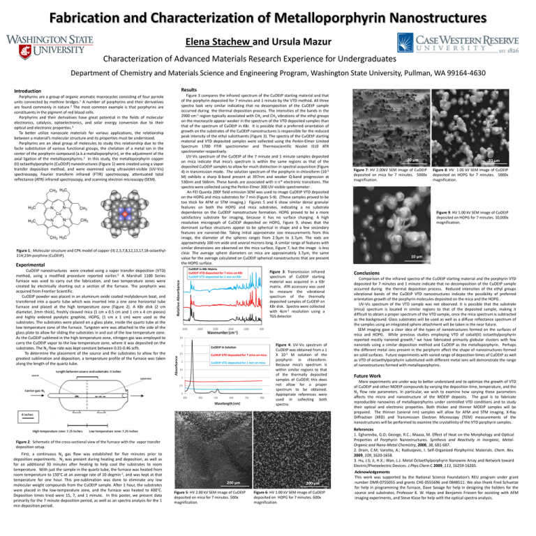
Fabrication and Characterization of Metalloporphyrin Nanostructures Elena Stachew and Ursula Mazur Characterization of Advanced Materials Research Experience for Undergraduates Department of Chemistry and Materials Science and Engineering Program, Washington State University, Pullman, WA 99164-4630 Introduction Porphyrins are a group of organic aromatic macrocycles consisting of four pyrrole units connected by methine bridges.1 A number of porphyrins and their derivatives are found commonly in nature.2 The most common example is that porphyrins are constituents in the pigment of red blood cells. Porphyrins and their derivatives have great potential in the fields of molecular electronics, catalysis, optoelectronics, and solar energy conversion due to their optical and electronic properties.3 To better utilize nanoscale materials for various applications, the relationship between a material’s molecular structure and its properties must be understood. Porphyrins are an ideal group of molecules to study this relationship due to the facile substitution of various functional groups, the chelation of a metal ion in the center of the porphyrin compound (a.k.a metalloporphyrin), or the adjustment of the axial ligation of the metalloporphyrins.2 In this study, the metalloporphyrin copper (II) octaethylporphyrin (CuOEtP) nanostructures (Figure 1) were created using a vapor transfer deposition method, and were examined using ultraviolet-visible (UV-Vis) spectroscopy, Fourier transform infrared (FTIR) spectroscopy, attentuated total reflectance (ATR) infrared spectroscopy, and scanning electron microscopy (SEM). Figure 1: Molecular structure and CPK model of copper (II) 2,3,7,8,12,13,17,18-octaethyl21H,23H-porphine (CuOEtP). Experimental CuOEtP nanostructures were created using a vapor transfer deposition (VTD) method, using a modified procedure reported earlier.3 A Marshall 1100 Series furnace was used to carry out the fabrication, and two temperature zones were created by electrically shorting out a section of the furnace. The porphyrin was acquired from Frontier Scientific. CuOEtP powder was placed in an aluminum oxide coated molybdenum boat, and transferred into a quartz tube which was inserted into a one zone horizontal tube furnace and placed at the high temperature zone (Figure 2). A KBr disk (2 cm diameter, 2mm thick), freshly cleaved mica (1 cm x 0.5 cm and 1 cm x 4 cm pieces) and highly ordered pyrolytic graphite, HOPG, (1 cm x 1 cm) were used as the substrates. The substrates were placed on a glass plate, inside the quartz tube at the low temperature zone of the furnace. Tungsten wire was attached to the side of the glass plate to allow for sliding the substrates in and out of the low temperature zone. As the CuOEtP sublimed in the high temperature zone, nitrogen gas was employed to carry the CuOEtP vapor to the low temperature zone, where it was deposited on the substrates. The N2 flow rate was kept constant between 0.35-0.46 scfh. To determine the placement of the source and the substrates to allow for the greatest sublimation and deposition, a temperature profile of the furnace was taken along the length of the quartz tube. Results Figure 3 compares the infrared spectrum of the CuOEtP starting material and that of the porphyrin deposited for 7 minutes and 1 minute by the VTD method. All three spectra look very similar indicating that no decomposition of the CuOEtP sample occurred during the thermal deposition process. The intensities of the bands in the 2900 cm-1 region typically associated with CH2 and CH3 vibrations of the ethyl groups on the macrocycle appear weaker in the spectrum of the VTD deposited samples than that of the spectrum of CuOEtP in KBr. It is possible that a preferred orientation of growth on the substrates of the CuOEtP nanostructures is responsible for the reduced peak intensity of the ethyl substituents (Figure 3). The spectra of the CuOEtP starting material and VTD deposited samples were collected using the Perkin-Elmer Limited Spectrum 1700 FTIR spectrometer and Thermoscientific Nicolet iS10 ATR spectrometer respectively. UV-Vis spectrum of the CuOEtP of the 7 minute and 1 minute samples deposited on mica indicate that mica’s spectrum is within the same regions as that of the deposited CuOEtP samples to allow for much distinction in spectral acquisition (Figure 4) in transmission mode. The solution spectrum of the porphyrin in chloroform (10-5 M) exhibits a sharp B-band present at 397nm and weaker Q-band progression at 530nm and 566nm. These bands are associated with -* electronic transitions. The spectra were collected using the Perkin-Elmer 300 UV-visible spectrometer . An FEI Quanta 200F field emission SEM was used to image CuOEtP VTD deposited on the HOPG and mica substrates for 7 min (Figure 5-9). (These samples proved to be too thick for AFM or STM imaging.) Figures 5 and 6 show similar dense granular features on both the HOPG and mica substrates, indicating a no substrate dependence on the CuOEtP nanostructure formation. HOPG proved to be a more satisfactory substrate for imaging, because it has no surface charging. A high resolution micrograph of CuOEtP deposited on HOPG, Figure 9, shows that the dominant surface structures appear to be spherical in shape and a few secondary features are nanorod-like. Taking initial approximate size measurements from this image, the diameter of the spheres ranges from 2.9µm to 3.7µm. The rods are approximately 100 nm wide and several microns long. A similar range of features with similar dimensions are observed on the mica surface, Figure 7, but the image is less clear. The average sphere diameters on mica are approximately 3.7µm, the same value for the average calculated on CuOEtP spherical nanostructures that are present the HOPG surface. CuOEtP in KBr Matrix CuOEtP VTD deposited for 7 mins on KBr CuOEtP VTD deposited for 1 min on KBr Figure 3: Transmission infrared spectrum of CuOEtP starting material was acquired in a KBr matrix. ATR accessory was used to measure the vibrational spectrum of the thermally deposited samples of CuOEtP on KBr disk. Spectra were collected with 4cm-1 resolution using a TGS detector. CuOEtP in Solution CuOEtP VTD deposited for 7 mins on mica CuOEtP VTD deposited for 1 min on mica Figure 4: UV-Vis spectrum of CuOEtP was obtained from a 1 X 10⁻⁵ M solution of the porphyrin in chloroform. Because mica’s spectrum is within similar regions to that of the thermally deposited samples of CuOEtP, this does not allow for a proper spectrum to be obtained. Appropriate references were used in collecting both spectra. Figure 2: Schematic of the cross-sectional view of the furnace with the vapor transfer deposition setup. First, a continuous N2 gas flow was established for five minutes prior to deposition experiments. N2 was present during heating and deposition, as well as for an additional 30 minutes after heating to help cool the substrates to room temperature. With just the sample in the quartz tube, the furnace was heated from room temperature to 150°C at an average rate of 10 degmin-1, and was kept at that temperature for one hour. This pre-sublimation was done to eliminate any low molecular weight compounds from the CuOEtP sample. After 1 hour, the substrates were placed in the low-temperature zone, and the furnace was heated to 400°C. Deposition times tried were 15, 7, and 1 minute. In this poster, we present data primarily for the 7 minute deposition period, as well as an spectra analysis for the 1 min deposition period. 200 µm Figure 5: HV 2.00 kV SEM image of CuOEtP deposited on mica for 7 minutes. 500x magnification. 200 µm Figure 6: HV 1.00 kV SEM image of CuOEtP deposited on HOPG for 7 minutes. 600x magnification. 20 µm 20 µm Figure 7: HV 2.00kV SEM image of CuOEtP deposited on mica for 7 minutes. 5000x magnification. 20 µm Figure 8: HV 1.00 kV SEM image of CuOEtP deposited on HOPG for 7 minutes. 5000x magnification. Figure 9: HV 1.00 kV SEM image of CuOEtP deposited on HOPG for 7 minutes. 10,000x magnification. 200 µm 10 µm Conclusions 200 µm Comparison of the infrared spectra of the CuOEtP starting material and the porphyrin VTD deposited for 7 minutes and 1 minute indicate that no decomposition of the CuOEtP sample occurred during the thermal deposition process. Reduced intensities of the ethyl groups vibrational bands of the CuOEtP VTD nanostructures indicate the possibility of preferred orientation growth of the porphyrin molecules deposited on the mica and the HOPG . UV-Vis spectrum of the VTD sample was not observed. It is possible that the substrate (mica) spectrum is located in similar regions to that of the deposited sample, making it difficult to obtain a proper spectrum of the VTD sample, once the mica spectrum is subtracted as the background. Glass substrates will be used as well as a diffuse reflectance spectrum of the samples using an integrated sphere attachment will be taken in the near future. SEM imaging gave a clear idea of the types of nanostructures formed on the surfaces of 10 µm mica and HOPG. While previous studies employing VTD of cobalt(II) octaethylporphyrin reported mostly nanorod growth,3 we have fabricated primarily globular clusters with few nanorods using a similar deposition method and CuOEtP as the metalloporphyrin. Perhaps the different metal ions present in the porphyrin affect the shape of nanostructures formed on solid surfaces. Future experiments with varied range of deposition times of CuOEtP as well as VTD of octaethylporphyrin substituted with different metal ions will demonstrate the range of nanostructures formed with metalloporphyrins. Future Work More experiments are under way to better understand and to optimize the growth of VTD of CuOEtP and other MOEtP compounds by varying the deposition time, temperature, and the N2 flow rate parameters. In particular, we wish to examine how varying these parameters affects the micro and nanostructure of the MOEtP deposits. The goal is to fabricate reproducible nanowires of metalloporphyrins under controlled VTD conditions and to study their optical and electronic properties. Both thicker and thinner MOEtP samples will be prepared. The thinner (several nm) samples will allow for AFM and STM imaging. X-Ray Diffraction (XRD) and Transmission Electron Microscopy (TEM) measurements of the nanostructures will be performed to examine the crystallinity of the VTD porphyrin samples. References 1. Egharevba, G.O; George, R.C.; Maaza, M. Effect of Heat on the Morphology and Optical Properties of Porphyrin Nanostructures. Synthesis and Reactivity in Inorganic, MetalOrganic and Nano-Metal Chemistry, 2008, 38, 681-687. 2. Drain, C.M; Varotto, A.; Radivojevic, I. Self-Organized Porphyrinic Materials. Chem. Rev. 2009, 109, 1620-1658. 3. Hu, J.S; Ji, H.X.; Wan, L.J. Metal Octaethylporphyrin Nanowire Array and Network toward Electric/Photoelectric Devices. J.Phys.Chem.C 2009, 113, 16259-16265. Acknowledgements This work was supported by the National Science Foundation’s REU program under grant number DMR-0755055 and grants CHE-0555696 and 0848511. We also thank Fred Schuetze for help in programming the furnace, Dave Savage for help in designing the holders for the source and substrates, Professor K. W. Hipps and Benjamin Friesen for assisting with AFM imaging experiments, and Steve Klase for help with the optical spectra analysis.


