Hot electron luminescence in ZnS alternating-current thin-film
advertisement
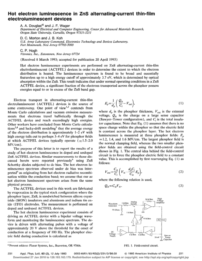
Hot electron luminescence electroluminescent devices in ZnS alternating-current thin-film A. A. Douglasa) and J. F. Wager Depnrtment of Electricui and Computer Engineering, Center for Advanced Materials Research, Owgon State LJniversity, Corvailis, Oregon 9733 l-321 1 D. C. Morton and J. El. Koh I,!S Army Luhorutory Command, Eiectrmics Fiirt il-lcnmczz~th,~NeioJemey 077O.MOOO Technology and Devices Laborutory, C. P. Hogh Fitronics, kc., Eaton tom, Neu) Jemy 07724 (Received 8 March 1993; accepted for publication 20 April 1993) Hot electron luminescence experiments are performed on ZnS aIt.ernating-current thin-film ele~tmluminescent (ACTFEL) devices in order to determine the extent to which the electron distribution is heated. The luminescence spectrum is found to be broad and essentially featureless up to a high energy cutoff of approximately 3.7 eV, which is determined by optical absorption within the ZnS. This result indicates that under normal operating conditions in a ZnS ACTFEZ. device, a significant fraction of the electrons transported across the phosphor possess energies equal to or in excess of the ZnS band gap. Electron transport in alternating-current thin-film eletctroluminescent (ACTFEL) devices is the source of some controversy. One point of view”’ contends from Monte G-10 calculations and vacuum emission measurements that electrons travel ballistically through the AC’?‘FEL device and reach exceedingly high energies. Other workers have concluded from Monte Carlo calculations”” and lucky-drift modelingS that the average energy of the electron distribution is approximately I-2 eV with high energy tails out to perhaps 3-A eV for phosphor fields at which ACTFEL devices typically operate ( z 1.5-2.0 MV~~Clll). The purpose of this letter is to report the results of a study of hot electron luminescence in doped and undoped ZnS ACTFIX. devices. Similar measurements to those discussed herein were reported previously” using ZnS Schottkg diodes subjected to tic bias. The hot electron luminescence spectrum observed under dc bias was interpreted” as originating from hot electron radiative recombin&ion within the conduction band; we assume that our ac hot electron luminescent spectrum arises from the same physical process. The -4ClTFE.L devices used in this work are fabricated by evaporation in the typical stack configuration where the phosphor layer7 ZnS, is sandwiched between silicon oxynitride (SiON) insulators and aluminum and iridium tin oxide (.LTO) electrodes. The measurement is performed on doped and undoped ACYFFEL devices. The hot electron luminescence experiment consists of driving an A<J”I‘FEL device with a bipolar voltage waveform and monitoring the luminescence spectrum. The device is driven with alternating pulses with a voltage of approximately 20 V above the threshold for the onset of conduction at a frequency of 100 Hz. The phosphor electric field during conduction is calculated as --.--~ ___ .~ ‘+%esetrt address: PIanar Systems, Inc., tleaverton, OR WW6. 231 fip=;( $--jL), where dp is the phosphor thickness, re.;,, is the external voltage, Qst is the charge on a large sense capacitor (Sawyer-Tower configuration), and Ci is the total insulator capacitance. Note that Eq. ( 1) assumes that there is no space charge within the phosphor so that the electric field is constant across the phosphor layer. The hot electron luminescence is measured at three phosphor fields: rP = 1.2, 1.3, and 1.6 MV/cm. The largest phosphor field is the normal clamping field, whereas the two smaller phosphor fields are obtained using the field-control circuit shown in Fig. 1. The central idea behind the field-control circuit is to force the phosphor electric field to a constant value. This is accomplished by first rearranging Eq. ( 1) as follows: cst F’s,---< d/Gql 3 Kxt=c, ( 1 where the following relation is used, (3) Qst= c,t j,‘,t * ,i%\ ,,g 0 LcMnl I)~ ‘:r>:~T~f;-& v0ttaE.t’ Supply ’ p& 1 sitw>er 50 111: ;i,, &W;<,, FIG, 1. Field-control circuit. AppS. Phys. Lett. 63 (21, 12 July 1993 0003.6951/93/63(2)/231/3/$6.00 0 1993 American Institute of Physics 231 Downloaded 27 Jan 2010 to 128.193.163.179. Redistribution subject to AIP license or copyright; see http://apl.aip.org/apl/copyright.jsp z.‘J 5 2 2 0 0.6 ‘S & 0.0 -0.5 -1.0 -1.5 -2.0 0.0 0 100 200 0.0 300 1.6 Time (microseconds) 2.0 2.4 2.8 3.2 3.6 4.0 Photon Energy (eV) FIG. 2. (a) Phosphor field and (b) luminescence transient curves at 460 nm. FIG. 4. Electron luminescence spectra at two emission angles at 1.6 MVlcm. Then, field control is achieved by realizing Ey. (2) using the circuit shown in Fig. 1. Since the goal of the fieldcontrol circuit is to hold E, constant, the last term in the parentheses is a constant; the magnitude of this constant is set by the dc bias, Ydcr indicated in Fig. 1. The prefactor multiplying the expression within the parentheses is the closed-loop gain of the field-control circuit which is equal to the ratio of C,, to Cj. The hot electron luminescent spectra are measured using a SPEX 3/4 meter monochrometer and a cooled, extended range photomultiplier tube (PMT). Specctraare obtained in a time-resolved manner by digitally acquiring the voltage across a 50 kQ resistor between the PMT and ground. A single-system correction to the rdw spectral data is performed which accounts for lens, grating, and detector response. Optical absorption measurements of the ACTFEL stack are performed using a SPEX Fluorolog System, which includes a xenon lamp and a pair of 0.22 m double monochrometers. Phosphor field and hot electron luminescence transient curves are shown in Fig. 2 for a wavelength of460 ntn. The first peak in the E,,(t) curve corresponds to the application of an external voltage pulse; note that field clamping occurs at approximately 1.6 MV/cm. The 1.4 MV/cm constant field portion of the E,(t) curve occurs when the fieldcontrol circuit is operational. Note that although the du- ration of the hot electron luminescence is very short (microseconds) and is concomitant with the flow of conduction current, the duration of the measured luminescence transient is approximately 100 ps, which is determined by the RC time constant of the 50 kI1 resistor and the PMT. Also, notice that the 1.4 MV/cm luminescence signal is weak compared to that of the first peak; we have found 1.2 h%V/cm to be the smallest phosphor field at which we can obtain adequate signal intensity with the present setup. Hot electron luminescence spectra are plotted in Fig. 3 for Ep= 1.2, 1.4, and 1.6 MV/cm. The structure observed in Fig. 3 is attributed to optical interference since these peaks shift, as shown in Fig. 4, when the emission angle of the sample is rotated by approximately 45” with respect to the monochrometer. cAs apparent from Fig. 3, the high energy, hot electron luminescence cutoff occurs at about 3.7 eV. Optical absorption spectra for the ACTFEL stack, the glass substrate, and IT0 on glass are given in Fig. 5. It is clear from Fig. 5 that the absorption edge at about 3.7 eV arises from absorption within the ZnS layer. Thus, a comparison of the hot electron luminescence spectra of Fig. 3 and the optical absorption spectra of Fig. 5 indicates that the high energy, hot electron luminescence cutoff arises from optical absorption within the ZnS layer. Therefore, if we correct for optical interference and absorption effects, the hot electron luminescence spectrum is I.0 1.0 2 & 0.8 2 ,$ 0.8 b ‘Z 0.6 f; g 0.3 g .H 2 0.2 FY 0.0 1 .‘\ip--q-- (a) \ v ,eJ-J@ (cry k-......... i _i_?s”:*~, -4 1.6 2.0 2-i 2.X 3.2 3.6 4.0 Photon Energy (rV) FIG. 3. Electron luminescence spectra for various phosphor fields: [a) 1.6 MVi’cm, (b) 1A MVicm, and (c) I.2 MV/cm. 232 Appl. Phys. Lett., Vol. 63, No. 2, 12 July 1993 fyy+, (,b) p . ,_._,lg-.k~. y,,.,.VT --*’ $;I ‘\ :\ \‘ :, i ka) (c)i I; ; 5, !\ ‘, --+-- ~ b .g 0.6 f 0.4 -s +j 0.2 p: 0.0 1.0 2.0 3.0 4.0 5,O Photon Ericr_q (cV) FIG. 5. Optical absorption spectra for (a) the glass substrate, (b) the glass substrate and the IT0 layer, and cc) the full ACTFEL stack. Douglas ei a/= 232 Downloaded 27 Jan 2010 to 128.193.163.179. Redistribution subject to AIP license or copyright; see http://apl.aip.org/apl/copyright.jsp broad and rather structureless out to energies approaching 3.7 eV, the band gap of ZnS. The hot electron luminescence spectrum arises from the radiative transition of energetic electroris within the ZnS conduction bandb and, therefore, is related to the hot electron distribution. Thus, we conclude that a significant fraction of the hot electrons transiting the ZnS possess kinetic energies near to, and most likely in excess of, the 3.7 eV band gap of ZnS. Moreover, although the intensity of the hot electron luminescence scales with the magnitude of the applied field, as indicated in Fig. 3, the shape of the hot electron luminescence spectrum is relatively independent of field. In prtrticular, the high energy tail extends out. to 3.7 eV for all of the fields investigated. This implies that for any field large enough to cause significant tunnel emission from interfaces states, a substantial number of the emitted dcctmns will reach ut ieast band-gap energies. We cannot infer anything about. the hot electron distribution for energies in excess of 3.7 eV since these energies are inaccessible to this experiment. Further attempts were made to optically measure the high energy tail of the eltztron emission. A sample was broken and edge emission monitored. The edge emission spectrum contains the Same 3.7 eV cutoff as before. This implies that the intensity of edge-emitted, high energy photons is so low that they are completely undetectable. Qne implication of the high energy of the electron distribution inferred from the hot electron luminescence experiment is that it now seems possible that band to band impact ionization occurs in these devices. The threshold energy for impact ionization, I&,, is given by,’ 21~1,+ in], - &, ErJa== m,+ f?lh where” q,= (9.343~ is the electron effective mass, mh = I .76?q is the heavy-hole eB?ctive mass, and &=3.7 eV is the band gap. This results in Eth of approximately 4.3 eV. Extrapolation of Fig. 3 suggests that band to band impact ionization would likely occur in ZnS ACTFEL devices under normal operating conditions. 233 Appl. Phys. h&t., Vol. 63, No. 2, 12 July 1993 A second implication of the work reported herein is that the achievement of efficient blue ACTFEL devices should not be impeded by the transport properties, if ZnS is employed as the host phosphor. Finally, it should be noted that although all of the data shown in this letter are for undopcd samples, the high energy portion of the hot electron luminescence spectrum is identical for Mn-doped samples, to within the accuracy of the experiment. Thus, the Mn luminescent impurities do not significantly cool the electron distribution. This result is consistent with the Monte Carlo simulation’ of Bhattacharyya et al., who found the Mn impact excitation scattering rate to be several orders of magnitude smaller than that of polar optical phonon or intervalley scattering. In conclusion, the hot electron luminescence spectrum is measured for an ACTFEL device in which the ZnS is grown by evaporation. The luminescence spectrum is broad and featureless and is cut OR‘at the ZnS band gap due to optical absorption. This result provides evidence that a substantial fraction of the electrons transiting the ACTFEL device have energies near to or in excess of the ZnS band gap. We wish to thank Ron Rhormaei of Planar Systems for providing samples. This work was supported by the U.S. Army Research Ofice under Contract DllL039160242 and the U.S. Army LABCOM under Contract DAALOl-39-C-0927 as administered by GE0 Centers, Inc. ‘R. Mach and G. 0. Miiller, J. Cryst. Growth 101, 967 (1990). ‘I-I. J. Fitting, G. 0. Miiller, R. Mach, G. LJ. Reinsperger, T. H. Hingst, and E. Schreiber, Phys. Status Solidi A 121, 305 ( 1990). 3K. Brennan, J. Appl. Phys. 64, 4024 (1988). ‘K. Bhattacharyya, S. M. Goodnick, and J. F. Wager, L’l~~c~rolumin~scence, edited by V. P. Singh and J. C. McClure, (Cinco Puntos, El Paso, TX, 1992), p. 54. ‘E. I3ringuicr, J. Appl. Phys. 70, 4505 ( 1991). “N. E. Rigby and J. W. Allm, J. Phys. C 21, 34S3 (1988). ‘C. M. Wolfe, N. Holonyak, Jr., and G. E. Stillman, P/IJJS&Z~ Projx~rci~~s ofSe/niconducmrr (Prentice IIall, Englewood Cliffs, NJ, 19891, p. 299. aLirn~lolt-B~~nzsreit!New Series (Springer, Berlin, 19X7), Vol. 22, pp. 167-168. “K. Bhattacharyya, S. M. Goodnick, and J. F. Wager, J. Appl. Phys. 73, 3390 (1993). Douglas et al. 233 Downloaded 27 Jan 2010 to 128.193.163.179. Redistribution subject to AIP license or copyright; see http://apl.aip.org/apl/copyright.jsp
