Efficiency of SiC JFET-Based Inverters Hui Zhang, Leon M. Tolbert
advertisement
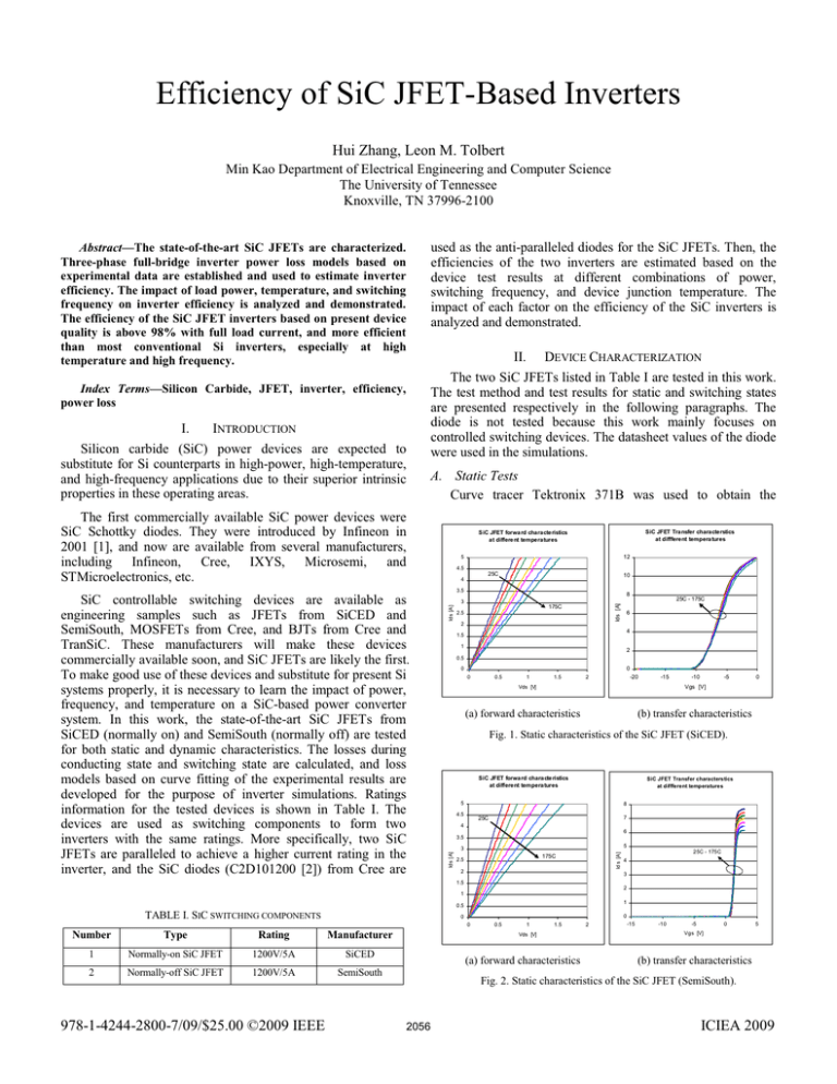
Efficiency of SiC JFET-Based Inverters Hui Zhang, Leon M. Tolbert Min Kao Department of Electrical Engineering and Computer Science The University of Tennessee Knoxville, TN 37996-2100 Abstract—The state-of-the-art SiC JFETs are characterized. Three-phase full-bridge inverter power loss models based on experimental data are established and used to estimate inverter efficiency. The impact of load power, temperature, and switching frequency on inverter efficiency is analyzed and demonstrated. The efficiency of the SiC JFET inverters based on present device quality is above 98% with full load current, and more efficient than most conventional Si inverters, especially at high temperature and high frequency. Index Terms—Silicon Carbide, JFET, inverter, efficiency, power loss I. INTRODUCTION Silicon carbide (SiC) power devices are expected to substitute for Si counterparts in high-power, high-temperature, and high-frequency applications due to their superior intrinsic properties in these operating areas. used as the anti-paralleled diodes for the SiC JFETs. Then, the efficiencies of the two inverters are estimated based on the device test results at different combinations of power, switching frequency, and device junction temperature. The impact of each factor on the efficiency of the SiC inverters is analyzed and demonstrated. II. DEVICE CHARACTERIZATION The two SiC JFETs listed in Table I are tested in this work. The test method and test results for static and switching states are presented respectively in the following paragraphs. The diode is not tested because this work mainly focuses on controlled switching devices. The datasheet values of the diode were used in the simulations. A. Static Tests Curve tracer Tektronix 371B was used to obtain the The first commercially available SiC power devices were SiC Schottky diodes. They were introduced by Infineon in 2001 [1], and now are available from several manufacturers, including Infineon, Cree, IXYS, Microsemi, and STMicroelectronics, etc. SiC JFET Tra nsfer characterstics at diffferent tempera tures SiC JFET forwa rd characteristics at differe nt temperatures 12 5 4.5 25C 4 10 3.5 Ids [A] Ids [A] 8 3 175C 2.5 25C - 175C 6 2 4 1.5 1 2 0.5 0 0 0 0.5 1 1.5 -20 2 -15 -10 -5 0 Vgs [V] Vds [V] (a) forward characteristics (b) transfer characteristics Fig. 1. Static characteristics of the SiC JFET (SiCED). SiC JFET forward characteristics at different temperatures SiC JFET Transfer characterstics at diffferent temperatures 5 8 4.5 7 25C 4 6 3.5 5 Ids [A] 3 Ids [A] SiC controllable switching devices are available as engineering samples such as JFETs from SiCED and SemiSouth, MOSFETs from Cree, and BJTs from Cree and TranSiC. These manufacturers will make these devices commercially available soon, and SiC JFETs are likely the first. To make good use of these devices and substitute for present Si systems properly, it is necessary to learn the impact of power, frequency, and temperature on a SiC-based power converter system. In this work, the state-of-the-art SiC JFETs from SiCED (normally on) and SemiSouth (normally off) are tested for both static and dynamic characteristics. The losses during conducting state and switching state are calculated, and loss models based on curve fitting of the experimental results are developed for the purpose of inverter simulations. Ratings information for the tested devices is shown in Table I. The devices are used as switching components to form two inverters with the same ratings. More specifically, two SiC JFETs are paralleled to achieve a higher current rating in the inverter, and the SiC diodes (C2D101200 [2]) from Cree are 175C 2.5 2 25C - 175C 4 3 1.5 2 1 1 0.5 TABLE I. SIC SWITCHING COMPONENTS 0 0 0 Number Type Rating Manufacturer 1 Normally-on SiC JFET 1200V/5A SiCED 2 Normally-off SiC JFET 1200V/5A SemiSouth 978-1-4244-2800-7/09/$25.00 ©2009 IEEE 0.5 1 1.5 Vds [V] (a) forward characteristics 2 -15 -10 -5 0 5 Vgs [V] (b) transfer characteristics Fig. 2. Static characteristics of the SiC JFET (SemiSouth). 2056 ICIEA 2009 SiC JFET switching loss SiC JFET switching loss 160 160 140 120 1A 100 2A 80 3A 60 4A 40 Energy Loss [1e-6 J] 140 Energy loss [1e-6 J] forward and transfer characteristics. The SiC JFETs are put into an environmental chamber to raise the ambient temperature up to 175 °C in 25 °C increments. The characteristics of the SiCED and SemiSouth devices are shown in Figs. 1 and 2, respectively. As shown as Fig. 1 and Fig. 2, the on-state resistance of the SiC JFETs increases with temperature from 25 °C to 175 °C, and transfer characteristics of the both devices are nearly constant at this temperature range. 120 100 80 25 60 75 40 5A 20 125 20 175 0 0 50 100 150 0 200 0 dc Thermal box 2 Temperature [C] L 4 6 Current [A] Fig. 6. Switching loss of the SiC JFET at different conditions (SiCED). + - Fig. 3. Switching test circuit. B. Switching Tests The test circuit shown in Fig. 3 is used for switching tests. It has a pure inductive load, and the switch is controlled by a double-pulse signal. The current in the switch is controlled by tuning the duty ratio of the first pulse. Commercial gate driver IC HCNW3120 is used to drive these devices. Different power supply voltages are given to meet the different gate signal needs of the devices. The gate signal waveforms when using a gate resistance of 10 are shown for SiCED and SemiSouth in Figs. 4 (a) and Fig. 5 (a), respectively. In addition, the devices are put into the chamber to raise the junction temperature up to 300 300 250 250 200 1A 2A 150 3A 4A 100 5A 50 Energy Loss [1e-6 J] IF SiC JFET switching loss SiC JFET Switching loss VF Energy loss [1e-6 J] DUT 200 150 25 100 75 125 50 175 0 0 0 50 100 150 200 0 2 Temperature [C] 4 6 Current [A] Fig. 7. Switching loss of the SiC JFET at different conditions (SemiSouth). 175 °C. The switching waveforms of the devices at the test condition of 200 V, 5 A and 175 °C are also shown in Figs. 4(b) and Fig. 5(b). Their switching energy losses at different temperature and different current level are shown in Fig. 6 (SiCED) and Fig. 7 (SemiSouth). All the switching losses increase with increasing current and are almost constant with increasing temperature. III. INVERTER POWER LOSS CALCULATION Inverter power loss is mainly composed of conduction power loss and switching power loss. A widely used averaging technique [3-6] is employed to study the inverter power loss. The primary algorithm is presented in this section. For more details, please see [7-8]. (a) gate signal waveforms (b) switching waveforms @ 175 °C A. Conduction power loss For SiC JFETs and MOSFETs, the conduction loss is mainly caused by on-state resistance, Ron. It is calculated by Fig. 4. Test waveforms of the SiC JFET (SiCED). Pcond = I rms 2 ⋅ Ron , (1) where Irms is the effective current flowing in the device. For an inverter under SPWM control, the effective current can be expressed as [8] I rms = I (a) gate signal waveforms (b) switching waveforms @ 175 °C 1 1 + M cos φ 8 3π , (2) where M is modulation index, I is the peak of phase current, and φ is the current phase angle with respect to voltage (The Fig. 5. Test waveforms of the SiC JFET (SemiSouth). 2057 TABLE II. RESISTANCE PARAMETERS OF THE SIC JFETS TABLE III. SWITCHING LOSS PARAMETERS OF THE SIC JFETS Device a b c Device d e f SiC JFET (SiCED) 0.0021 0.5981 141.57 SiC JFET (SiCED) 0.9932 -3.6578 22.755 SiC JFET (SemiSouth) 0.0054 0.3457 107.43 SiC JFET (SemiSouth) 1.14 -1.9954 30.211 phase current is i = I sin(θ - φ), and only fundamental is considered.). Therefore, the conduction power loss is 1 1 ! Pcond = I 2 Ron " + M cos φ # $ 8 3π %. where d, e, f are coefficients which are obtained from the curve fitting of the experimental data in Figs. 6 and 7 (see Table III). Then, substitute (6) into (5) to obtain (7), an expression of the effective switching power loss based on test data. (3) Ron = aT 2 + bT + c (mΩ) . (4) The on-state resistances are shown in Fig. 8 and curve fitting determines the parameters in (4). The a, b, and c coefficients of the two devices are summarized in Table II. In addition, Fig. 8 also indicates that the conduction loss of the SiC JFET from On-state re sistance s of the SiC JFETs (7) Effective switching energy loss of the SiC JFETs 140 350 Resistance [miliohm] ! I # ( !W ) , % The switching energy losses for the devices computed by (7) are shown in Fig. 9. As shown in Fig. 9, the SiC JFET from SiCED is more efficient in terms of switching losses. Energy loss [1e-6J] As shown in Fig. 1 and Fig. 2, the values of Ron are functions of device junction temperatures. By letting the on resistance be a quadratic function of current, it can be represented by 2d 3 e 2 f Psw = f sw ⋅ Esw = f sw ⋅ " I + I + 4 π $ 3π 120 SemiSouth 100 80 60 40 SiCED 20 0 0 300 4 6 8 10 12 Current [A] SiCED 250 2 200 Fig. 9. Effective switching energy loss of the SiC JFETs. SemiSouth 150 100 0 50 100 150 IV. 200 Temperature [C] Fig. 8. On-state resistances of the SiC JFETs. SemiSouth is lower at room temperature, while at the temperatures above 150 °C, the SiC JFET from SiCED is better in terms of conduction loss. B. Switching power loss By [7], the effective switching energy loss of a SPWM controlled inverter is expressed as Esw = 1 2π 2π +φ , & E (θ ) dθ (5) φ if phase current is i = I sin(θ - φ). Further, the switching energy loss is a function of current at a certain temperature by the test results (see Figs. 6 and 7), and does not change much for different temperatures. So neglecting the influence of temperature, it can be expressed as a polynomial function of current as E (i ) = di 3 + ei 2 + fi (!J) , (6) 2058 INVERTER POWER LOSS CALCULATIONS Based on the discussions in the previous section, the efficiency for a three phase full bridge inverter based on each of the two SiC JFETs is determined for different operation conditions using MATLAB Simulink. Assume DC bus voltage is 480 V, output voltage fundamental frequency is 60 Hz, and the load is an RL load (R=23.81 , L=0.0015 H), which makes current in the devices reach 10 A at modulation index M=1. A. At different load powers Assume the junction temperature is 50 °C and switching frequency is 10 kHz. The modulation index is varied to change the load current from 0 to 10 A, and the power losses for different load currents are calculated. The efficiencies of the inverters based on the two different devices are shown in Fig. 10. The efficiency increases with load power and reaches a maximum at M=1. The maximum efficiency of each inverter is 99.0% for the SiCED JFET inverter and 98.8% for the SemiSouth JFET inverter. Generally, the efficiency of Si inverters ranges from 93% to 97% at rated power. So the two SiC JFET inverters are more efficient than most Si inverters. In addition, the losses of the SiC JFETs dominate the total inverter losses, and unlike the diodes, the switching losses are larger than the conduction losses in the two SiC JFETs. Efficiencies of the SiC JFET inverters at different power levels 1.00 Efficiencies of the SiC JFET inverters at different temperatures 0.995 SiCED Efficiency Efficieny 0.99 0.98 SemiSouth 0.97 SiCED 0.990 0.985 SemiSouth 0.980 0.96 0.975 0.95 0 0.5 1 1.5 2 2.5 3 3.5 25 4 75 125 175 Temperature [C] Load power [kW] Fig.10. Efficiencies of the SiC inverters at different load powers. Fig.12. Efficiencies of the SiC inverters at different temperatures. B. At different switching frequencies Assume the junction temperature is 50 °C and the load current is 10 A. Increase the switching frequency to 50 kHz and compute the power losses. As expected, the efficiencies of the inverters decrease with the switching frequency as shown in Fig. 11. The efficiencies of the two SiC JFET inverters decrease slightly with increased switching frequency, and keep relatively high values even at 50 kHz (97.1% for SiCED inverter and 95.6% for SemiSouth inverter). The switching frequency of 50 kHz is not possible for most high power Si power devices due to the extreme high power loss and demanding cooling requirements. inverter can be substituted by a naturally or forced convection heatsink depending on power involved. V. CONCLUSIONS The SiC JFET inverters have relatively high efficiency at all powers, switching frequency, and temperature ranges. Compared to Si inverters, the advantage is more obvious at high frequency and high temperature. Motion control, solar energy, wind generation, and vehicle systems might benefit from these SiC inverters in the near future. Finally, the SiC JFETs presented in this paper are not commercial products. Thus, with more development of SiC semiconductor technology, the efficiency of inverters based on future SiC products will be further improved. Efficiencies of the SiC JFET inverters at different switching frequencies REFERENCES 1.00 Efficiency [1] SiCED 0.99 [2] 0.98 0.97 SemiSouth [3] 0.96 0.95 0 10 20 30 40 50 Switching frequency [kHz] [4] Fig.11. Efficiencies of the SiC inverters at different switching frequencies. C. At different junction temperatures Assume the load current is 10 A and switching frequency is 10 kHz. Raise the junction temperature to 175 °C and calculate the inverter losses. As shown in Fig. 12, the efficiencies of the SiC inverters decrease only slightly with increasing temperature. The difference of the efficiencies from 25 °C to 175 °C is less than 0.4% for both the inverters. Compared to Si inverters, the efficiency of the SiC inverters is much less sensitive to temperature. This implies that the thermal management system for SiC-based converters will be simpler. For example, a complex liquid-cooled heatsink used for a Si 2059 [5] [6] [7] [8] Silicon Carbide diode (C2D10120, 1200V/10A) datasheet, Cree, http://www.cree.comproducts/pdf/C2D10120.pdf. M. Holz, G. Hultsch, T. Scherg, R. Rupp, “Reliability considerations for recent Infineon SiC diode releases,” Microelectronics Reliability, vol. 47, Issues 9-11, Sep.-Nov. 2007, pp. 1741-1745. J.S. Lai, R.W. Young, G.W. Ott, Jr., J.W. McKeever, “Efficiency modeling and evaluation of a resonant snubber based soft-switching inverter for motor drive applications,” 26th Annual IEEE Power Electronics Specialists Conference, vol. 2, June 18-22, 1995, pp. 943949. M.H. Bierhoff, F.W. Fuchs, “Semiconductor losses in voltage source and current source IGBT converters based on analytical derivation,” IEEE 35th Annual Power Electronics Specialists Conference, vol. 4, 2004, pp. 2836-2842. F. Blaabjerg, U. Jaeger, S. Munk-Nielsen, “Power losses in PWM-VSI inverter using NPT or PT IGBT devices,” IEEE Transactions on Power Electronics, vol. 10, no. 3, May 1995, pp. 358-367. B. Ozpineci, L. M. Tolbert, S. K. Islam, M. Hasanuzzaman, “Effects of silicon carbide (SiC) power devices on PWM inverter losses,” The 27th Annual Conference of the IEEE Industrial Electronics Society, Nov.Dec., 2002, Denver, Colorado, pp. 1061-1066. H. Zhang, “Electro-thermal modeling of SiC power electronic systems,” Ph.D. Dissertation of the University of Tennessee, 2007. H. Zhang, M. Chinthavali, B. Ozpineci, L. M. Tolbert, "Power losses and thermal modeling of 4H-SiC VJFET inverter," IEEE Industry Applications Society Annual Meeting, October 2-6, 2005, Hong Kong, China, pp. 2630-2634.
