Reflective measurements of SiC
advertisement
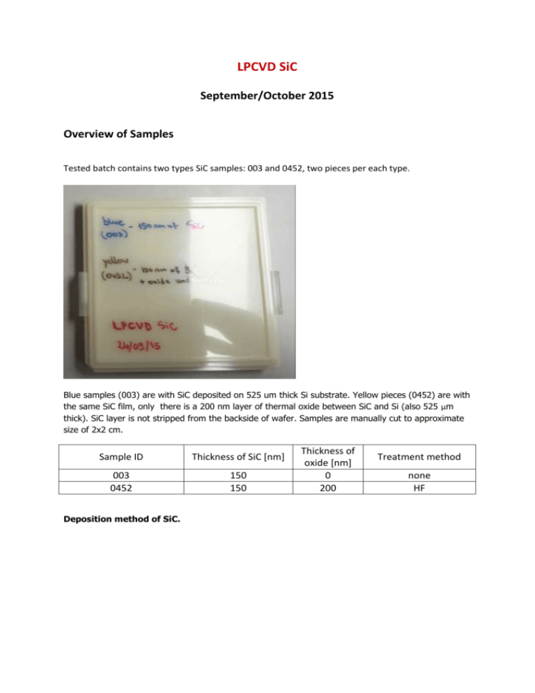
LPCVD SiC September/October 2015 Overview of Samples Tested batch contains two types SiC samples: 003 and 0452, two pieces per each type. Blue samples (003) are with SiC deposited on 525 um thick Si substrate. Yellow pieces (0452) are with the same SiC film, only there is a 200 nm layer of thermal oxide between SiC and Si (also 525 μm thick). SiC layer is not stripped from the backside of wafer. Samples are manually cut to approximate size of 2x2 cm. Sample ID Thickness of SiC [nm] 003 0452 150 150 Deposition method of SiC. Thickness of oxide [nm] 0 200 Treatment method none HF Measurements of SEY in Photonis The measurements were done at the same conditions as previous run (basic vacuum 7E-11 mbar, 20 nA e-beam, 3-4 mm dia.). Fig.1 and Fig.2 is for non-treated samples (just after loading to the system). Samples of each type are named as ‘’L’’ and ‘’R’’, according to the position in a received box. For SiC samples with SiO2 layer underneath small charging is observed. The SY curves are about the same for all samples. After that one of SiC sample was heat-cleaned at 500 °C for 1 hour (blue curve, Fig.3) and after that AH treatment at RT (in the same vacuum setup) was applied to the sample (green curve). Heat-cleaning had no effect for SY. After AH-treatment the SY was slightly dropped.

