Matched Monolithic Dual Transistor MAT01 Data Sheet
advertisement
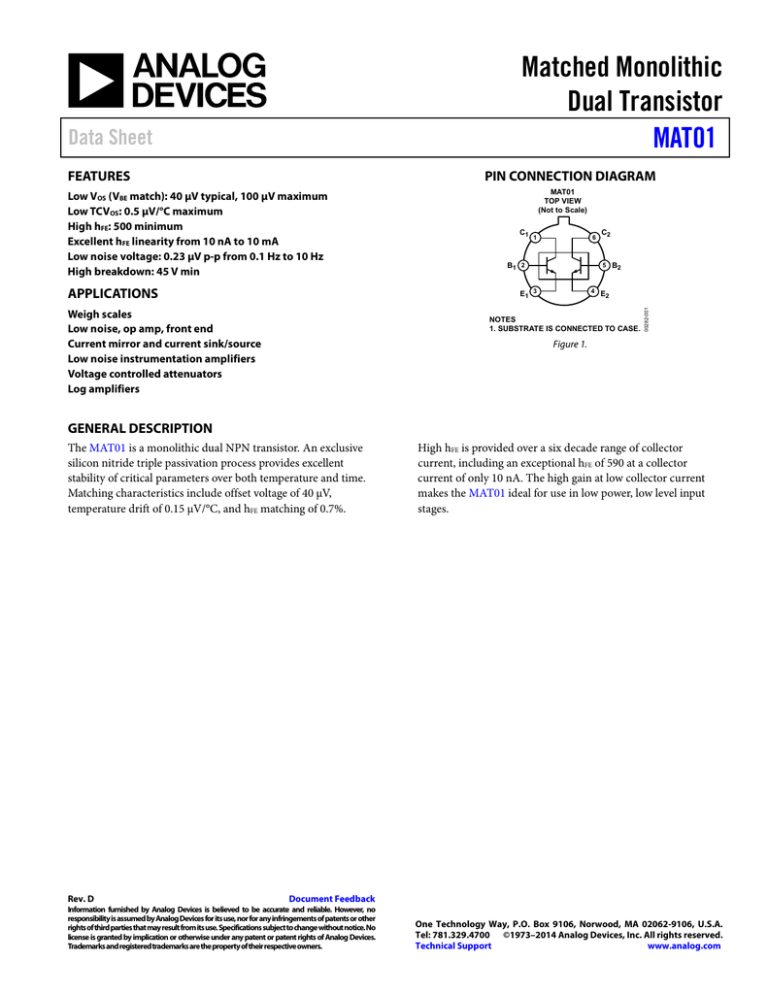
Matched Monolithic Dual Transistor MAT01 Data Sheet PIN CONNECTION DIAGRAM Low VOS (VBE match): 40 µV typical, 100 µV maximum Low TCVOS: 0.5 µV/°C maximum High hFE: 500 minimum Excellent hFE linearity from 10 nA to 10 mA Low noise voltage: 0.23 µV p-p from 0.1 Hz to 10 Hz High breakdown: 45 V min APPLICATIONS MAT01 TOP VIEW (Not to Scale) C1 1 6 5 B2 B1 2 4 E 2 E1 3 Weigh scales Low noise, op amp, front end Current mirror and current sink/source Low noise instrumentation amplifiers Voltage controlled attenuators Log amplifiers C2 NOTES 1. SUBSTRATE IS CONNECTED TO CASE. 00282-001 FEATURES Figure 1. GENERAL DESCRIPTION The MAT01 is a monolithic dual NPN transistor. An exclusive silicon nitride triple passivation process provides excellent stability of critical parameters over both temperature and time. Matching characteristics include offset voltage of 40 µV, temperature drift of 0.15 µV/°C, and hFE matching of 0.7%. Rev. D High hFE is provided over a six decade range of collector current, including an exceptional hFE of 590 at a collector current of only 10 nA. The high gain at low collector current makes the MAT01 ideal for use in low power, low level input stages. Document Feedback Information furnished by Analog Devices is believed to be accurate and reliable. However, no responsibility is assumed by Analog Devices for its use, nor for any infringements of patents or other rights of third parties that may result from its use. Specifications subject to change without notice. No license is granted by implication or otherwise under any patent or patent rights of Analog Devices. Trademarks and registered trademarks are the property of their respective owners. One Technology Way, P.O. Box 9106, Norwood, MA 02062-9106, U.S.A. Tel: 781.329.4700 ©1973–2014 Analog Devices, Inc. All rights reserved. Technical Support www.analog.com MAT01 Data Sheet TABLE OF CONTENTS Features .............................................................................................. 1 ESD Caution...................................................................................5 Applications ....................................................................................... 1 Typical Performance Characteristics ..............................................6 Pin Connection Diagram ................................................................ 1 Test Circuits........................................................................................8 General Description ......................................................................... 1 Applications Information .................................................................9 Revision History ............................................................................... 2 Typical Applications ....................................................................... 10 Specifications..................................................................................... 3 Outline Dimensions ....................................................................... 11 Electrical Characteristics ............................................................. 3 Ordering Guide .......................................................................... 11 Absolute Maximum Ratings ............................................................ 5 REVISION HISTORY 9/14—Rev. C to Rev. D 2/02—Rev. A to Rev. B Changes to Figure 4 and Figure 7 ................................................... 6 Edits to Features.................................................................................1 Deleted Wafer Test Limits ................................................................3 Deleted DICE Characteristics ..........................................................3 Edits to Table 5 ...................................................................................7 4/13—Rev. B to Rev. C Updated Format .................................................................. Universal Added Applications Section, Deleted Figure 2, Renumbered Sequentially................................................................ 1 Deleted Table 3, Renumbered Sequentially................................... 4 Changes to Table 3 ............................................................................ 5 Changes to Typical Performance Characteristics Section ........... 6 Updated Outline Dimensions ....................................................... 11 Changes to Ordering Guide .......................................................... 11 Rev. D | Page 2 of 12 Data Sheet MAT01 SPECIFICATIONS ELECTRICAL CHARACTERISTICS VCB = 15 V, IC = 10 µA, TA = 25°C, unless otherwise noted. Table 1. Parameter VOLTAGE Breakdown Voltage Offset Voltage Offset Voltage Stability First Month1 Long Term2 CURRENT Offset Current Bias Current Current Gain Current Gain Match NOISE Low Frequency Noise Voltage Broadband Noise Voltage Noise Voltage Density OFFSET VOLTAGE/CURRENT Offset Voltage Change Offset Current Change LEAKAGE Collector to Base Leakage Current Collector to Emitter Leakage Current Collector to Collector Leakage Current SATURATION Collector Saturation Voltage GAIN BANDWIDTH PRODUCT CAPACITANCE Output Capacitance Collector to Collector Capacitance Symbol Test Conditions/Comments Min BVCEO VOS IC = 100 µA 45 MAT01AH Typ Max 0.1 VOS/Time 2.0 0.2 IOS IB hFE 0.1 13 590 770 840 0.7 0.8 0.6 20 ∆hFE 500 MAT01GH Typ Min 45 0.04 IC = 10 nA IC = 10 µA IC = 10 mA IC = 10 µA 100 nA ≤ IC ≤ 10 mA Min 0.10 0.5 2.0 0.2 250 3.0 Unit V mV µV/Mo µV/Mo 0.2 18 430 560 610 1.0 1.2 3.2 40 nA nA 8.0 % % 0.4 9.0 7.6 7.5 µV p-p µV rms nV/√Hz nV/√Hz nV/√Hz en p-p en rms en 0.1 Hz to 10 Hz3 1 Hz to 10 kHz fO = 10 Hz3 fO = 100 Hz3 fO = 1000 Hz3 0.23 0.60 7.0 6.1 6.0 0.4 9.0 7.6 7.5 0.23 0.60 7.0 6.1 6.0 ∆VOS/∆VCB ∆IOS/∆VCB 0 ≤ VCB ≤ 30 V 0 ≤ VCB ≤ 30 V 0.5 2 3.0 15 0.8 3 8.0 70 µV/V pA/V ICBO ICES ICC VCB = 30 V, IE = 04 VCE = 30 V, VBE = 04, 5 VCC = 30 V5 15 50 20 50 200 200 25 90 30 200 400 400 pA pA pA VCE(SAT) 0.12 0.8 450 0.20 0.12 0.8 450 0.25 fT IB = 0.1 mA, IC = 1 mA IB = 1 mA, IC = 10 mA VCE = 10 V, IC = 10 mA V V MHz COB CCC VCB = 15 V, IE = 0 VCC = 0 2.8 8.5 1 2.8 8.5 pF pF Exclude first hour of operation to allow for stabilization. Parameter describes long-term average drift after first month of operation. 3 Sample tested. 4 The collector to base (ICBO) and collector to emitter (ICES) leakage currents can be reduced by a factor of 2 to 10 times by connecting the substrate (package) to a potential that is lower than either collector voltage. 5 ICC and ICES are guaranteed by measurement of ICBO. 2 Rev. D | Page 3 of 12 MAT01 Data Sheet VCB = 15 V, IC = 10 µA, −55°C ≤ TA ≤ +125°C, unless otherwise noted. Table 2. Parameter OFFSET VOLTAGE/CURRENT Offset Voltage Average Offset Voltage Drift1 Offset Current Average Offset Current Drift2 BIAS CURRENT CURRENT GAIN LEAKAGE CURRENT Collector to Base Leakage Current Collector to Emitter Leakage Current Collector to Collector Leakage Current ( Symbol Test Conditions/Comments VOS TCVOS IOS TCIOS ΙΒ hFE ICBO ICES ICC Min 167 TA = 125°C, VCB = 30 V, IE = 03 TA = 125°C, VCE = 30 V, VBE = 01, 3 TA = 125°C, VCC = 30 V1 ) MAT01AH Typ Max 0.06 0.15 0.9 10 28 400 0.15 0.50 8.0 90 60 15 50 30 80 300 200 Min 77 MAT01GH Typ Min 0.14 0.35 1.5 15 36 300 0.70 1.8 15.0 150 130 mV µV/°C nA pA/°C nA 25 90 50 200 400 400 nA nA nA V Guaranteed by VOS test TCVOS ≅ OS for VOS <<VBE , T = 298 K for TA = 25°C. T 2 Guaranteed by IOS test limits over temperature. 3 The collector to base (ICBO) and collector to emitter (ICES) leakage currents can be reduced by a factor of 2 to 10 times by connecting the substrate (package) to a potential that is lower than either collector voltage. 1 Rev. D | Page 4 of 12 Unit Data Sheet MAT01 ABSOLUTE MAXIMUM RATINGS Stresses above those listed under Absolute Maximum Ratings may cause permanent damage to the device. This is a stress rating only; functional operation of the device at these or any other conditions above those indicated in the operational section of this specification is not implied. Exposure to absolute maximum rating conditions for extended periods may affect device reliability. Table 3. 1 Parameter Breakdown Voltage of Collector to Base Voltage (BVCBO) Collector to Emitter Voltage (BVCEO) Collector to Collector Voltage (BVCC) Emitter to Emitter Voltage (BVEE) Emitter to Base Voltage (BVEBO)2 Current Collector (IC) Emitter (IE) Total Power Dissipation Case Temperature ≤ 40°C3 Ambient Temperature ≤ 70°C4 Temperature Range Operating Junction Storage Lead Temperature (Soldering, 60 sec) Rating 45 V 45 V 45 V 45 V 5V ESD CAUTION 25 mA 25 mA 1.8 W 500 mW −55°C to +125°C −55°C to +150°C −65°C to +150°C 300°C 1 Absolute maximum ratings apply to packaged devices. Application of reverse bias voltages in excess of rating shown can result in degradation of hFE and hFE matching characteristics. Do not attempt to measure BVEBO greater than the 5 V rating. 3 Rating applies to applications using heat sinking to control case temperature. Derate linearity at 16.4 mW/°C for case temperatures above 40°C. 4 Rating applies to applications not using heat sinking; device in free air only. Derate linearity at 6.3 mW/°C for ambient temperatures above 70°C. 2 Rev. D | Page 5 of 12 MAT01 Data Sheet TYPICAL PERFORMANCE CHARACTERISTICS OFFSET VOLTAGE (µV) OV < VCB < 30V 150 MAT01G 100 MAT01A 0 –75 00282-002 50 0 –25 50 25 75 100 125 10 8 6 DEVICE B 2 0 DEVICE C –2 DEVICE D –4 –6 –8 –10 150 DEVICE A 4 00282-005 ABSOLUTE CHANGE IN OFFSET VOLTAGE (µV) 200 0 1 3 2 5 4 TEMPERATURE (°C) 7 6 9 8 10 11 12 13 TIME (Months) Figure 2. Offset Voltage vs. Temperature Figure 5. Offset Voltage vs. Time 1000 1000 MAT01A MAT01A 800 CURRENT GAIN (hfe) CURRENT GAIN (hFE) 800 MAT01G 600 400 MAT01G 600 0 1n 10n 100n 1µ 10µ 100µ 1m 10m 100nA < IC < 25mA OV < VCB < 30V (EXCLUDES ICBO ) 00282-003 TA = 25°C VCB = 15V 200 –75 100m –50 –25 Figure 3. Current Gain vs. Collector Current 50 75 100 125 Figure 6. Current Gain vs. Temperature 1000 100 TA = 25°C 100 10 IC = 10µA WORST CASE IC = 300µA TYPICAL 1 10 100 10k 00282-004 IC = 10µA TYPICAL 10 IC = 10µA WORST CASE IC = 10µA TYPICAL 0.1 0.1 10k IC = 300µA TYPICAL 1 00282-007 NOISE CURRENT DENSITY (pA/√Hz) TA = 25°C NOISE VOLTAGE DENSITY (nV/√Hz) 25 TEMPERATURE (°C) COLLECTOR CURRENT (A) 1 0.1 0 00282-006 400 200 1 10 100 1k FREQUENCY (Hz) FREQUENCY (Hz) Figure 4. Noise Voltage Density vs. Frequency Figure 7. Noise Current Density vs. Frequency Rev. D | Page 6 of 12 10k Data Sheet MAT01 1000 10µA 1µA Δ < 0.1mV 100nA 10nA 1nA Δ < 0.3mV 100pA 10pA 0 100 Δ ≈ DEVIATION FROM STRAIGHT LINE 200 300 400 500 600 700 00282-008 COLLECTOR CURRENT (IC) Δ < 0.3mV 100µA 800 BASE TO EMITTER VOLTAGE (mV) Figure 8. Collector Current vs. Base to Emitter Voltage 10 TA = +125°C TA = +25°C TA = –55°C 0.1 00282-009 SATURATION VOLTAGE (V) MAT01 IC = 10 × IB 0.01 0.01 0.1 1 10 COLLECTOR CURRENT (mA) TA = 25°C VCE = 10V 200 100 MAT01 50 20 10 5 2 1 1µA 10µA 100µA 1mA COLLECTOR CURRENT (IC) 10mA Figure 10. Unity-Gain Bandwidth vs. Collector Current 100 1 500 00282-010 MAT01 TA = 25°C 1mA UNITY-GAIN BANDWIDTH PRODUCT (MHz) 10mA 100 Figure 9. Saturation Voltage vs. Collector Current Rev. D | Page 7 of 12 100mA MAT01 Data Sheet TEST CIRCUITS +16.5V +16.5V 50kΩ* 20kΩ 50kΩ* 50kΩ* VOUT OP1177 100kΩ 1% S1B 1MΩ 100pF UNITS CLOSED CLOSED IOS 1MΩ* MAT01 VOS S1B S1A TEST –15V S1A OPEN OPEN VOUT1 1V PER mV VOUT2 – VOUT1 1V PER nA 100kΩ 1% 100pF 00282-011 20µA V– *MATCHED TO 0.01% Figure 11. Matching Measurement Circuit +15V 50kΩ* 50kΩ* +15V 50kΩ* S3 A S2 S1A S1B 4MΩ –15V 3.3kΩ 2.5MΩ 4MΩ MAT01 B SPECTRUM ANALYZER OR QUAN-TECH IC NOISE ANALYZER 2181/2283 4kΩ V01 NOISE DENSITY V02 LOW FREQUENCY NOISE 4.7µF 2pF 2pF 720kΩ 100Ω 20µA –15V S1A S1B S3** READING NOISE VOLTAGE DENSITY CLOSED CLOSED CLOSED (PER TRANSISTOR) A V01/√2 NOISE CURRENT DENSITY (PER TRANSISTOR) CLOSED A V01/(√2 × 4MΩ) OPEN B V02 PEAK-TO-PEAK 25,000 TEST LOW FREQUENCY NOISE (REFERRED TO INPUT) OPEN OPEN CLOSED CLOSED S2 **A AND B REFER TO THE THROW POSITION OF THE SWITCH Figure 12. Noise Measurement Circuit Rev. D | Page 8 of 12 00282-012 *MATCHED TO 0.01% Data Sheet MAT01 APPLICATIONS INFORMATION Application of reverse bias voltages to the emitter to base junctions in excess of ratings (5 V) may result in degradation of hFE and hFE matching characteristics. Check circuit designs to ensure that reverse bias voltages above 5 V cannot be applied during transient conditions, such as at circuit turn-on and turn-off. Stray thermoelectric voltages generated by dissimilar metals at the contacts to the input terminals can prevent realization of the predicted drift performance. Maintain both input terminals at the same temperature, preferably close to the temperature of the device package. Rev. D | Page 9 of 12 MAT01 Data Sheet TYPICAL APPLICATIONS 1mA VREF Q1 Q2 R1 1.5kΩ NOTES 1. R1 MAY BE ADJUSTED TO MINIMIZE TCVREF . INCREASING R1 CAUSES A POSITIVE CHANGE IN TCVREF. 2. hFE OF Q1 IS REDUCED BY OPERATION OF BREAKDOWN MODE. 00282-013 VREF ≈ 7.0V TCVREF ≈ 100ppm/°C RO ≈ 40Ω Figure 13. Precision Reference UP TO 100 FEET CABLE +15V –15V DIFFERENTIAL AMPLIFIER AND CURRENT SOURCES °C K EO –55°C = 218K = 2.18V +25°C = 298K = 2.98V +125°C = 398K = 3.98V EO = 10mV/K 3-DIGIT DPM 0V TO +10V FULL SCALE 00282-014 SENSING PAIR MAT01H Figure 14. Basic Digital Thermometer Readout in Degrees Kelvin (K) SENSING PAIR MAT01H +15V DIFFERENTIAL AMPLIFIER AND CURRENT SOURCES HIGH 2.73V + POWER SUPPLY – METER DISPLAYS EO –2.73V –15V LOW EO = 10mV/K 2 1/2 DIGIT DPM BIPOLAR DIFFERENTIAL INPUTS –55°C = –0.55V +25°C = +0.25V +125°C = +1.25V Figure 15. Digital Thermometer with Readout in °C Rev. D | Page 10 of 12 00282-015 UP TO 100FT. CABLE Data Sheet MAT01 OUTLINE DIMENSIONS 0.185 (4.70) 0.165 (4.19) REFERENCE PLANE 0.750 (19.05) 0.500 (12.70) 0.250 (6.35) MIN 0.100 (2.54) BSC 0.050 (1.27) MAX 0.160 (4.06) 0.110 (2.79) 5 0.335 (8.51) 0.305 (7.75) 0.370 (9.40) 0.335 (8.51) 4 0.200 (5.08) BSC 3 6 0.045 (1.14) 0.027 (0.69) 2 0.019 (0.48) 0.016 (0.41) 0.040 (1.02) MAX 0.045 (1.14) 0.010 (0.25) 1 0.100 (2.54) BSC 0.034 (0.86) 0.027 (0.69) 0.021 (0.53) 0.016 (0.41) 45° BSC CONTROLLING DIMENSIONS ARE IN INCHES; MILLIMETER DIMENSIONS (IN PARENTHESES) ARE ROUNDED-OFF INCH EQUIVALENTS FOR REFERENCE ONLY AND ARE NOT APPROPRIATE FOR USE IN DESIGN. 022306-A BASE & SEATING PLANE Figure 16. 6-Pin Metal Header Package [TO-78] (H-06) Dimensions shown in inches and (millimeters) ORDERING GUIDE Model1 MAT01AH MAT01AHZ MAT01GH MAT01GHZ 1 VOS Maximum (TA = 25°C) 0.1 mV 0.1 mV 0.5 mV 0.5 mV Temperature Range −55°C to +125°C −55°C to +125°C −55°C to +125°C −55°C to +125°C Package Description 6-Pin Metal Header Package [TO-78] 6-Pin Metal Header Package [TO-78] 6-Pin Metal Header Package [TO-78] 6-Pin Metal Header Package [TO-78] Z = RoHS Compliant Part. Rev. D | Page 11 of 12 Package Option H-06 H-06 H-06 H-06 MAT01 Data Sheet NOTES ©1973–2014 Analog Devices, Inc. All rights reserved. Trademarks and registered trademarks are the property of their respective owners. D00282-0-9/14(D) Rev. D | Page 12 of 12
