a Engineer To Engineer Note EE-205
advertisement
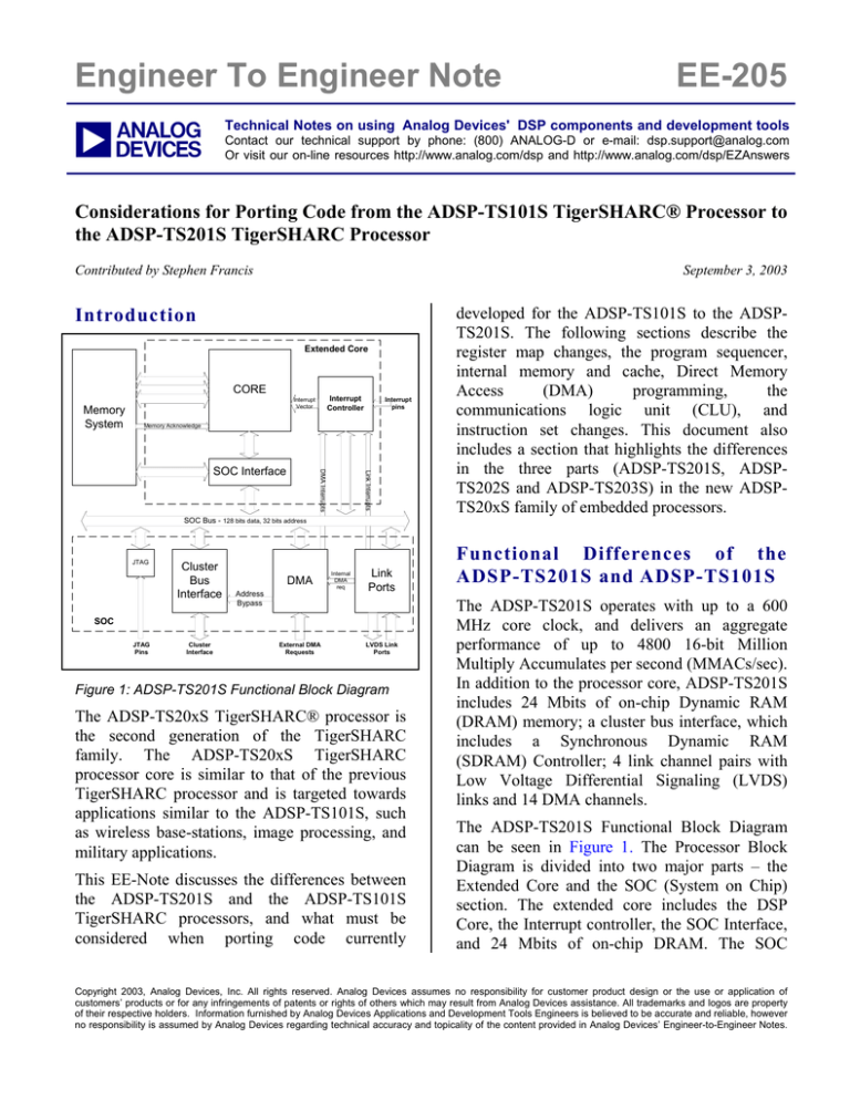
Engineer To Engineer Note EE-205 Technical Notes on using Analog Devices' DSP components and development tools a Contact our technical support by phone: (800) ANALOG-D or e-mail: dsp.support@analog.com Or visit our on-line resources http://www.analog.com/dsp and http://www.analog.com/dsp/EZAnswers Considerations for Porting Code from the ADSP-TS101S TigerSHARC® Processor to the ADSP-TS201S TigerSHARC Processor Contributed by Stephen Francis September 3, 2003 Introduction Extended Core CORE Memory System Interrupt Controller Interrupt Vector Interrupt pins Memory Acknowledge Link Interrupts DMA Interrupts SOC Interface SOC Bus - 128 bits data, 32 bits address JTAG Cluster Bus Interface DMA Address Bypass Internal DMA req Link Ports SOC JTAG Pins Cluster Interface External DMA Requests LVDS Link Ports Figure 1: ADSP-TS201S Functional Block Diagram The ADSP-TS20xS TigerSHARC® processor is the second generation of the TigerSHARC family. The ADSP-TS20xS TigerSHARC processor core is similar to that of the previous TigerSHARC processor and is targeted towards applications similar to the ADSP-TS101S, such as wireless base-stations, image processing, and military applications. This EE-Note discusses the differences between the ADSP-TS201S and the ADSP-TS101S TigerSHARC processors, and what must be considered when porting code currently developed for the ADSP-TS101S to the ADSPTS201S. The following sections describe the register map changes, the program sequencer, internal memory and cache, Direct Memory Access (DMA) programming, the communications logic unit (CLU), and instruction set changes. This document also includes a section that highlights the differences in the three parts (ADSP-TS201S, ADSPTS202S and ADSP-TS203S) in the new ADSPTS20xS family of embedded processors. Functional Differences of the ADSP-TS201S and ADSP-TS101S The ADSP-TS201S operates with up to a 600 MHz core clock, and delivers an aggregate performance of up to 4800 16-bit Million Multiply Accumulates per second (MMACs/sec). In addition to the processor core, ADSP-TS201S includes 24 Mbits of on-chip Dynamic RAM (DRAM) memory; a cluster bus interface, which includes a Synchronous Dynamic RAM (SDRAM) Controller; 4 link channel pairs with Low Voltage Differential Signaling (LVDS) links and 14 DMA channels. The ADSP-TS201S Functional Block Diagram can be seen in Figure 1. The Processor Block Diagram is divided into two major parts – the Extended Core and the SOC (System on Chip) section. The extended core includes the DSP Core, the Interrupt controller, the SOC Interface, and 24 Mbits of on-chip DRAM. The SOC Copyright 2003, Analog Devices, Inc. All rights reserved. Analog Devices assumes no responsibility for customer product design or the use or application of customers’ products or for any infringements of patents or rights of others which may result from Analog Devices assistance. All trademarks and logos are property of their respective holders. Information furnished by Analog Devices Applications and Development Tools Engineers is believed to be accurate and reliable, however no responsibility is assumed by Analog Devices regarding technical accuracy and topicality of the content provided in Analog Devices’ Engineer-to-Engineer Notes. a includes the External cluster bus interface, the Link ports, the DMA controller and the JTAG emulation port. The ADSP-TS201S is a functional variant of the TigerSHARC family, with some enhancements to the previous processor core’s internal units and bus system, memory organization and external link ports. Because the cores of the ADSP-TS201S and ADSP-TS101S processors are functionally identical, they both can execute the same instructions, along with some additional instructions that the ADSP-TS201 can execute, the XCORRS operation for example. Flag pins, have been added to the Sequencer on the ADSP-TS201S. The registers that are moved to the Interrupt Control block are the ILAT (low and high with set and clear addresses), IMASK (low and high), PMASK (low and high), the TIMER (0 and 1, low and high) and TMRIN registers (0 and 1, low and high). The ILAT, IMASK and PMASK registers have the same bit definitions as on the ADSP-TS101S with a few exceptions. The differences can be seen in Figure 2 and Figure 3. Register Map Changes Changes in the Extended Core include modifications in the register map. Some of the registers are on the SOC agents and others are in the core. Changes to the register map are highlighted in the following sub-sections, and a summary table (Table 1) of the bit definition register changes is provided at the end of this section. For more details on the register map, please refer to the Memory and Register Map Chapter (Chapter 2) in the ADSP-TS201 TigerSHARC Processor Hardware Reference Manual, and also the defTS201.h system header file that is installed with the TigerSHARC VisualDSP++™ development tools (C:\Program Files\Analog Devices\VisualDSP\TS\include). Note: System Header Files, such as defTS201.h, are used to declare global definitions, especially memory mapped registers, system architecture and processors. Sequencer register files Some of the registers that were part of the Sequencer on the ADSP-TS101S now become part of the Interrupt Controller on the ADSPTS201S. A number of the remaining registers in the Sequencer have some bit definition changes, and some new registers, for the operation of the Figure 2: IMASKH, ILATH, PMASKH (Upper) Register Bits on the ADSP-TS101S Figure 3: IMASKH, ILATH, PMASKH (Upper) Register Bits on the ADSP-TS201S These changes in the ILAT, IMASK and PMASK registers are only in the ILATH, IMASKH and PMASKH (upper) registers, and so only these sections of the ILAT, IMASK and PMASK registers are shown here. The remainder of the ILAT, IMASK and PMASK registers are unchanged in the ADSP-TS201S. Considerations for Porting Code from the ADSP-TS101S TigerSHARC® Processor to the ADSP-TS201S TigerSHARC Processor (EE-205) Page 2 of 14 a There are a number of bit definition changes in the Sequencer Control (SQCTL) Register on the ADSP-TS201S, compared to the ADSP-TS101S. Figure 4: SQCTL (Upper) Register Bits on the ADSPTS101S The Flag bits, located at bits 27-20 in the SQCTL register on the ADSP-TS101S (Figure 4) have been moved to the new FLAGREG register on the ADSP-TS201S (see Figure 10). Figure 5: SQCTL (Upper) Register Bits on the ADSPTS201S The Edge/Level interrupt control bits, located at bits 19-16 in the SQCTL register on the ADSPTS101S (Figure 4) have been moved to the interrupt control (INTCTL) register in the Interrupt Controller Block on the ADSP-TS201S, Figure 11. Bits 27-16 in the SQCTL register are now reserved on the ADSP-TS201S as can be seen in Figure 5. register in the Interrupt Controller on the ADSPTS201S (Figure 11). The Exception and Global Interrupt Enable bits (IMASK: bits 62 and 60 in the ADSP-TS101S, Figure 2) have been removed from the IMASK register and have been added to the SQCTL register on the ADSP-TS201S (bits 3 and 2 respectively in Figure 7). The Emulation bit (IMASK: bit 63 in the ADSP-TS101S, Figure 2) has been removed from the IMASK register and now the EMEN bit in the EMUCTL register includes this functionality. Figure 7: SQCTL (Lower) Register Bits on the ADSPTS201S The BTB lock (BTBLK) and BTB enable (BTBEN) bits located at bits 1-0 in the SQCTL register on the ADSP-TS101S (Figure 6) have been moved to the SQSTAT register on the ADSP-TS201S and are controlled by new instructions. There are a number of bit definition changes in the Sequencer Status (SQSTAT) Register on the ADSP-TS201S, compared to the ADSP-TS101S. Figure 8: SQSTAT (Upper) Register Bits on the ADSP-TS101S Figure 6: SQCTL (Lower) Register Bits on the ADSPTS101S The Timer Control bits, located at bits 13-12 in the SQCTL register on the ADSP-TS101S (Figure 6) have also been moved to the INTCTL The BTBEN and BTBLK bits, which have been moved from the SQCTL register (Figure 6), are located at bits 28 and 29 respectively in the SQSTAT register on the ADSP-TS201S (Figure 9). BTBEN is set while the BTB is enabled. When BTBLK is set, every new entry is put into Considerations for Porting Code from the ADSP-TS101S TigerSHARC® Processor to the ADSP-TS201S TigerSHARC Processor (EE-205) Page 3 of 14 a the BTB with the lock bit set. The Emulation, Exception and HW interrupt bits have been removed from the PMASK register and have been added to the SQSTAT register (bits 22, 21 and 20 respectively) on the ADSP-TS201S (Figure 9). addresses), IMASK (low and high), PMASK (low and high), the TIMER (0 and 1, low and high), and TMRIN registers (0 and 1, low and high). Figure 9: SQSTAT (Upper) Register Bits on the ADSP-TS201S The ILATSTL register is used to set a bit in ILATL, while the ILATCLL register is used to clear a bit in ILATL. Likewise, The ILATSTH register is used to set a bit in ILATH, while the ILATCLH register is used to clear a bit in ILATH. New registers have been added to the Sequencer for the operation of the Flag Pins. The Flag (FLAGREG) register, Figure 10, contains the Flag direction and Flag value bits that have been removed from the SQCTL register (bits 27-20 in SQCTL on the ADSP-TS101). The bits to control the direction of the Flag pins (3-0) are located at bits 3-0 respectively. The Flag value bits for the Flag pins (3-0) are located at bits 7-4 respectively. Note: the FLGx bits do not change location and are located in the SQSTAT register on both the ADSP-TS101S and the ADSPTS201S. The FLAGREGST register is used to set a bit in FLAGREG, while the FLAGREGCL register is used to clear a bit in FLAGREG. Figure 10: FLAGREG (Lower) Register Bits on the ADSP-TS201S Interrupt Control Registers The Interrupt Controller register block on the ADSP-TS201S includes a number of registers that have been moved from the Sequencer on the ADSP-TS101. The registers that have been moved to the Interrupt Control block are the ILAT (low and high with set and clear The bit definitions of the ILATL, IMASKL and PMASKL registers do not change in the ADSPTS201S relative to the ADSP-TS101S, while bit definitions of the ILATH, IMASKH and PMASKH registers are identical to the ADSPTS101S, except for the bits that have been moved to the SQCTL and SQSTAT registers (Bits 31:28), as described previously. Figure 11: INTCTL (Lower) Register Bits on the ADSP-TS201S The INTCTL register, Figure 11, on the ADSPTS201S contains the Edge/Level interrupt control bits and the Timer Control bits, which have been moved from the SQCTL register, as described previously. The Edge/Level interrupt control bits for IRQ3-0 are located at bits 3-0 respectively. The Timer Control bits, TMR1RN and TMR0RN, are located at bits 5-4 respectively. The remainder of the INTCTL register is reserved. External Interface Registers There are changes in the Link port registers relative to the ADSP-TS101S. The link ports on the ADSP-TS201S are similar to those on the ADSP-TS101S in the way they are accessed by the core and the DMA, but different in their physical implementation. Figure 12 and Figure Considerations for Porting Code from the ADSP-TS101S TigerSHARC® Processor to the ADSP-TS201S TigerSHARC Processor (EE-205) Page 4 of 14 a 13 highlight the differences in the basic link port configuration. Note, the link ports on the ADSPTS201S are not compatible with previous TigerSHARC processor or SHARC DSP link ports. defined on the ADSP-TS101S. Additional registers are added to reflect the additional receive and transmit capability of the link ports, ie., the link receive and link transmit control registers (LRCTLx, LTCTLx) the link receive status and receive status clear registers (LRSTATx, LRSTATCx), and the transmit status and transmit status clear registers (LTSTATx, LTSTATCx). Please refer to the defts201.h header file for the bit definitions for the above link port registers. Figure 12: ADSP-TS101S Minimal Link Port Configuration – No Buffering Bit Function Register Changes Summary The ADSP-TS201S’s four full-duplex link ports each provide additional four-bit receive and fourbit transmit I/O capability, using Low-Voltage, Differential-Signal (LVDS) technology. With the ability to operate at a double data rate—latching data on both the rising and falling edges of the clock – running at 500 MHz, each link port can support up to 500M bytes per second per direction, for a combined maximum throughput of 4G bytes per second. Figure 13: ADSP-TS201S Minimal Link Port Configuration – No termination indicated Additional pins are provided for the Link ports on the ADSP-TS201S, as can be seen in Figure 13. For the hardware connection guidelines for the links ports on the ADSP-TS201S, please refer to EE-179 - ADSP-TS201S Hardware System Design Guidelines. The link buffer registers, LBUFTXx, LBUFRXx, (“x” stands for channel number 3:0) are as The following table (Table 1) gives a summary of the bit definitions that change registers from the ADSP-TS101S to the ADSP-TS201S. FUNCTION ADSP-TS101S Register ADSP-TS201S Register (BIT Locations) (BIT Locations) FLAGx_OUT SQCTL – (27-24) FLAGREG – (7-4) FLAGx_EN SQCTL – (23-20) FLAGREG – (3-0) IRQx_EDGE SQCTL – (19-16) INTCTL – (3-0) TMRxRN SQCTL – (13-12) INTCTL – (5-4) BTBLK SQCTL – (1) SQSTAT – (29) BTBEN SQCTL – (0) SQSTAT – (28) EMUL (IMASK) IMASKH – (63) EMEN bit in EMUCTL includes this functionality EXCEPT (IMASK) IMASKH – (62) SQCTL – (3) GIE (IMASK) IMASKH – (60) SQCTL – (2) EMUL (PMASK) PMASKH – (63) SQSTAT – (22) EXCEPT (PMASK) PMASKH – (62) SQSTAT – (21) GIE (PMASK) PMASKH – (60) SQSTAT – (20) Table 1: Summary of bit definition register changes. Considerations for Porting Code from the ADSP-TS101S TigerSHARC® Processor to the ADSP-TS201S TigerSHARC Processor (EE-205) Page 5 of 14 a ADSP-TS101S: Fetch 1 Hit/Miss check Fetch 2 Fetch 3 Decode Integer Operand BTB miss and Jump decision branch taken IALU & LC Execute1 Execute2 Jump decision COMPUTE ADSP-TS201S: Fetch 1 Fetch 2 Fetch 3 Hit/Miss check Fetch 4 PreDecode Decode Integer BTB miss and Jump decision branch taken IALU & LC Operand Execute1 Execute2 Jump decision COMPUTE Figure 14: Program Sequencer Pipeline changes Program Sequencer There are changes in the Program sequencer on the ADSP-TS201S, relative to the ADSPTS101S (see Figure 14). These changes are transparent to the user in that they do not have any impact on actual source code compatibility, but just on the actual cycle count due to the two new pipeline stages. Two new pipeline stages have been added, so the program sequencer on the ADSP-TS201S now consists of a ten-cycle instruction pipeline, ie., a four-cycle fetch pipe and a six-cycle execution pipe, with computation results available two cycles after operands are available. The memory access in the ADSP-TS201S is 4 cycles compared to 3 cycles in the ADSPTS101S. In order to comply with the longer memory access, another pipeline stage is added. Operations carried out in the Fetch 3 stage in the ADSP-TS101S are now carried out in the Fetch 4 stage in the ADSP-TS201S. The other new pipeline stage that has been added is the Pre-Decode stage, which is after the Fetch 4 stage and before the Decode stage. The PreDecode stage has been added to allow more time for the instruction alignment and instruction decoding. As in the ADSP-TS101S, the ADSP-TS201S supports branch prediction and includes a 128- entry branch target buffer (BTB) to reduce branch delays for efficient execution of conditional and unconditional branch instructions and zero-overhead looping; correctly predicted branches that are taken occur with zero overhead cycles, overcoming the five-to-nine stage branch penalty. This compares to the three-to-six stage branch penalty on the ADSP-TS101S. Note: As is the case with the ADSP-TS101, the pipeline for the ADSP-TS201S is fully interlocked, so when a dependency condition or resource conflict occurs the processor automatically inserts stalls. A stall is any delay that is caused by one of the two aforementioned conditions. This is fully transparent to the user, however since this may cause performance loss, the user should strive to create as few of these conditions as possible. Internal memory / Cache The internal memory of the ADSP-TS201S has a collective capacity of 24-Mbits of internal DRAM, compared with 6-Mbits of internal SRAM on the ADSP-TS101S. This is divided into 6 separate memory units with each memory block consisting of a 4-Mbit block of internal DRAM memory space, configured as 128K x 32bit words; each unit contains a memory crossbar that connects the unit to the extended core busses, as can be seen in Figure 15. Considerations for Porting Code from the ADSP-TS101S TigerSHARC® Processor to the ADSP-TS201S TigerSHARC Processor (EE-205) Page 6 of 14 a Figure 16: Memory Block Physical structure Figure 15: Internal DRAM Structure Each 4-Mbit internal DRAM memory block is divided into two half blocks, Half-Block 0 and Half-Block 1, and each half-block is created from two interleaved 1-Mbit sub-arrays, SubArrays 0 and 1 and respectively Sub-Arrays 2 and 3. A sub-array is partitioned into 512 pages of 2048 bits each, and each page holds eight 256bit words. The sub-arrays of a half-block are interleaved on a page basis. For more information on the Internal Memory of the ADSP-TS201S, please refer to the Memory and Buses Chapter (chapter 9) in the ADSPTS201S TigerSHARC Processor Programming Reference Manual. Accessing Internal Memory As stated previously, the internal memory of the ADSP-TS201S is divided into 6 separate memory units with a collective capacity of 24Mbits. Each unit contains a memory interface, a 4-Mbit segment of internal DRAM and a memory crossbar that connects the unit to the extended core busses (see Figure 16 for the physical structure of a memory block). The internal DRAM clock (DCLK) operates at ½ the frequency of the core clock (CCLK). To compensate for the slower clock speed, the internal DRAM utilizes a fundamental word size that is twice the width of the extended core busses, i.e. 256 bits. Also note that the internal DRAM is single ported. It can accommodate a single read or write transaction each memory clock cycle (DCLK). The penalties associated with accessing internal DRAM are variable and influenced by multiple factors. Understanding the origins of the penalties is critical when developing strategies to minimize the impact on processing efficiency. A simple, high-level overview of the internal DRAM access procedure provides a general guideline of when penalties occur and how they may be avoided. Reading from or writing to internal DRAM necessitates activating or opening the appropriate page of internal DRAM. Activating a page is the process of transferring a page of data from an internal DRAM sub-array to the corresponding page buffer. The procedure requires a single memory clock cycle (two core clock cycles). Once the page has been activated, a 256-bit word may be read from or written to the page buffer. Considerations for Porting Code from the ADSP-TS101S TigerSHARC® Processor to the ADSP-TS201S TigerSHARC Processor (EE-205) Page 7 of 14 a A read transaction will transfer a 256-bit word from the page buffer to a page of the prefetch buffer. Similarly, a write transaction will transfer a 256-bit word from the copyback buffer to the page buffer. This procedure also requires a single memory clock cycle (two core clock cycles). Activating a Page (1 DCLK or 2 CCLK cycles) Internal DRAM Page x Sub-Array y 256 bit word transfer (1 DCLK or 2 CCLK cycles) Page Buffer 256 bits Page of Prefetch Buffer refresh period CACMD_REFRESH into the CACMDALL function of the core clock at the beginning of the user’s program. This refresh period obviously depends on the processor’s core clock frequency. When the cycle count reaches the set value, the refresh takes place immediately without interrupting a page access (page prefetch or copyback sequence within the same page are completed before refresh). Note: there may be a latency if refreshes and accesses occur in the same memory block. Reading process from Internal DRAM 256 bit word transfer (1 DCLK or 2 CCLK cycles) Activating a Page (1 DCLK or 2 CCLK cycles) Internal DRAM Page x Sub-Array y Page Buffer 256 bits Page of Copyback Buffer Writing process to Internal DRAM Figure 17: Internal DRAM Read/Write Process Finally, a page must be closed or pre-charged before a different page in the same sub-array may be activated. Pre-charging a page is the process of transferring the page of data in a page buffer back into the internal DRAM. Any modifications made to the data of the page buffer will be reflected in the internal DRAM. Again, the procedure requires a single memory clock cycle (two core clock cycles). Figure 17 shows the Internal DRAM read/Write process. Internal DRAM Refresh In addition to standard read and write transactions, the internal DRAM must periodically refresh each page of memory. Refreshing a page is simply the process of activating a page and subsequently pre-charging the same page. The process is required because the basic memory cell of the internal DRAM utilizes a capacitor for storing data. Over time the capacitor can discharge and the contents of the memory can be lost. The refresh process periodically recharges the capacitor and ensures the data remains accurate. The user must set the Cache Module The cache module is composed of the cache data unit and the cache control unit. The cache control unit decodes the address of each memory transaction, and determines if the transaction is a cache hit or miss. If a transaction is a cache hit, the corresponding cache entry is either read from or written to the cache without penalty. However, if the transaction is a cache miss a penalty may be incurred. The penalty is suffered only if data must be read from or written to the internal DRAM. A cache miss on a read transaction that qualifies as a prefetch buffer hit or read buffer hit will not require a read from internal DRAM, and hence will not incur a penalty. Similarly, a cache miss on a write transaction that does not force a cache copyback will not require an internal DRAM write, and hence no penalty will be incurred. Buffer Module The buffer module, which serves to queue data read from or written to memory in an effort to reduce the frequency of read and write accesses to the internal DRAM, contains three distinct sets of buffers: the read buffer, the prefetch buffer, and the copyback buffer. The read buffer, a 512-bit buffer organized as two 256-bit words – one for each half-block is, Considerations for Porting Code from the ADSP-TS101S TigerSHARC® Processor to the ADSP-TS201S TigerSHARC Processor (EE-205) Page 8 of 14 a utilized for read transactions only and functions as the sole interface connecting the memory cross bar to the cache and the prefetch buffer for all read transactions. Note: data is never read from the internal DRAM directly. Instead it is copied to the prefetch buffer before subsequently being moved to the read buffer. If a transaction is a read buffer hit, no penalty is incurred. The prefetch buffer, an 8192-bit buffer organized as four 2048-bit pages (each page is parsed into eight 256-bit words), is utilized in read transactions only, and serves as an intermediate storage location for data read from internal DRAM before it is transferred to the read buffer. However, the primary function of the prefetch buffer is to anticipate sequential read transactions, and queue data from the internal DRAM in advance of the actual transaction requests. A prefetch buffer hit incurs no penalties. The copyback buffer, organized as two separate 4096-bit dual-page buffers, with each dual-page buffer accommodating sixteen 256-bit entries serves as an intermediate holding location for replaced cache entries that must eventually be written back to the internal DRAM. Note the copyback buffer is the sole interface to the internal DRAM for all write transactions. The utilization of an intermediate buffer versus an immediate write to internal DRAM is extremely beneficial. It provides a mechanism for delaying write accesses to internal DRAM. By delaying the write access, pending read transactions may be allowed to complete without incurring a penalty. The duration of the delay is limited only by the size of the buffer and how quickly the buffer is filled. Memory Crossbar blocks. In one cycle on the ADSP-TS101, up to three 128-bit transfers can occur within the core (two data transfers, and one program instruction transfer). The extended core of the ADSP-TS201S Processor includes four 128-bit busses: S-Bus, JBus, K-Bus, and I-Bus. The S-Bus accommodates internal memory transactions initiated by the SOC bus interface unit. The JBus accommodates internal memory transactions initiated by the JALU. The K-Bus accommodates internal memory transactions initiated by the KALU. The I-Bus accommodates internal memory transactions initiated by the sequencer. All of the extended core busses operate at core clock frequency (CCLK). At 600 MHz, the maximum core clock frequency, the extended core busses can support a combined throughput of 38.4 Gbytes/sec. The memory crossbar functions as a bridge that connects the four extended core busses to the individual memory units. It can support four transactions every core clock cycle, or more specifically one transaction per bus per cycle. The transaction size may be 32-bit word, 64-bit long word, or 128-bit quad word. Note the memory crossbar is the only interface to internal memory. Individual memory units can accommodate only a single transaction per core clock cycle. An arbitration procedure resolves conflicts when multiple transactions targeted to the same memory unit are initiated in the same cycle. Transaction priority order from highest to lowest is as follows: S-Bus transactions, J-Bus transactions, K-Bus transactions, and finally IBus transactions. Any transaction initiated but delayed in the previous cycle is prioritized higher than transactions initiated in the current cycle. The ADSP-TS101S has three internal memory blocks each consisting of 2M bits of memory space. There are three separate internal 128-bit data buses, each connected to one of the memory Considerations for Porting Code from the ADSP-TS101S TigerSHARC® Processor to the ADSP-TS201S TigerSHARC Processor (EE-205) Page 9 of 14 a Accessing Internal Guidelines Summary memory: Programming In summary, the internal DRAM read/write process is facilitated by the cache and buffer modules. The objective of this structure is to avoid stalls when the user’s program is being executed. Two methods of accessing the internal memory are recommended for effective use of internal memory in certain applications: sequential access and local access. The sequential access technique consists of sequentially accessing the internal memory. Only the very first access in the sequence is penalized because the page buffer is empty. Then, after this first access, the accesses are penalty free. This technique is very effective when applied to large blocks of memory and few accesses to the same data are performed. If possible, the user should not use the same memory segment for other accesses. Instead, the user should place the program code in one segment of internal memory and data variables in another. Also, the user should not access the same segment more than once in a single instruction. The local address technique consists of singular accesses to the internal memory, usually when data must be read or written. Because the first access is always penalized if the page buffer is empty, the user should try to apply the sequential access technique to access the internal memory or, preload the data into the cache in advance. This operation can be done at the beginning of the program, by reading and writing back the data block or by using the Direct Memory Access (DMA) controller. Or the cache can be locked and so the critical data block is preserved in the cache ready for future accesses. This technique is recommended for data blocks smaller than the cache size (4K words). processor, or by the (external) TigerSHARC processor bus master. The DMA operation is programmed by writing to the memory-mapped DMA Transfer Control Block (TCB) registers. Each TCB register is 128 bits long and is divided into four 32-bit registers: an Index register (DI), an X dimension count and increment register (DX), a Y dimension count and increment register (DY), and a Control and chaining pointer (DP). Figure 18: DP register on the ADSP-TS101S There some changes in the bits fields in the control and chaining pointer (DP) register on the ADSP-TS201S compared to the ADSP-TS101S. The DP register contains all the control information for the DMA. This register is split into two main fields. The first contains all the control information and the second the chaining information. The DP register on the ADSPTS101S is shown in Figure 18. The DP register on the ADSP-TS201S is shown in Figure 19. Note: the CHPT field includes bits 18–0 (bits 15–0 not shown). DMA Programming DMA operations can be programmed by the TigerSHARC processor core, by an external host Considerations for Porting Code from the ADSP-TS101S TigerSHARC® Processor to the ADSP-TS201S TigerSHARC Processor (EE-205) Page 10 of 14 a applied in non-communications algorithms. The CLU is highlighted in Figure 20. Figure 19: DP register on the ADSP-TS201S The MS (Memory select for the chain pointer) bits in the DP register on the ADSP-TS101S have been removed and the chain pointer bit field (CHPT) has been increased to adapt to the larger memory map on the ADSP-TS201S. The Chaining Destination Channel (CHTG) bit field has been reduced from 5 bits (21-17) on the ADSP-TS101S to 3 bits (21-19) on the ADSPTS201S. This means that the chaining to other channels that was allowed on the ADSP-TS101S is no longer allowed on the ADSP-TS201S. Figure 20: CLU in Compute Block X For more information on the DP register and setting up DMA Transfers, please refer to the Direct Memory Access chapter in the ADSPTS201S Processor Hardware Reference Manual. The XCORRS instruction correlates long input sequence (such as 2048 complex input numbers of an 8 bit pilot) with a known reference sequence for multiple delays. The XCORRS instruction can be viewed as a single-cycle execution of 16 parallel DESPREAD instructions. Some important features of the XCORRS instruction include: Communications Logic Unit The ADSP-TS201S processor core contains two computation units known as compute blocks. Each compute block contains a register file and the following independent computation units— an ALU, a multiplier, and a shifter. Each compute block also includes a new unit, the Communications Logic Unit (CLU). The CLU includes the ADSP-TS101S’s enhanced instructions for communications infrastructure to govern Trellis Decoding (Viterbi and Turbo decoders, for example), Despreading via complex correlations and a new operation, the Cross Correlations Function (XCORRS) which has been added on the ADSPTS201S. Note: these functions may also be The CLU takes its inputs from the register file, and returns its outputs to the register file. Most CLU instructions operate on the trellis registers (TR) and trellis history registers (THR). The accelerator register files are extended to 32 registers in the case of the TR register file (vs. 16 in the ADSP-TS101S) and the THR register file is extended to 4 registers (vs. 2 in the ADSPTS101S). • Clear (CLR) option, providing a mechanism to clear the trellis registers before beginning a new cross correlation. • Cut inputs (CUT) option, providing a mechanism to discard some input data numbers (for initial and final cycles; lower and upper triangles). • Extended-precision (EXT) option, supporting 16-bit input and 32-bit accumulation (instead of the default 8-bit input and 16-bit accumulation. • Outputs correlation strength for each delay Considerations for Porting Code from the ADSP-TS101S TigerSHARC® Processor to the ADSP-TS201S TigerSHARC Processor (EE-205) Page 11 of 14 a • Memory usage; execution considers memory bandwidth and access to multiple blocks Note: The Communications Logic Unit is available on the ADSP-TS201S only. No CLU instructions are included on the ADSP-TS202S and ADSP-TS203S, except for the Permute instruction, which is included on the ADSPTS202S and ADSP-TS203S. Instruction set and instruction functionality changes The following section describes the changes in the instruction set and functionality. Virtual Bus Transactions When a transaction occurs between registers or between external memory and a register, it can be executed on any internal bus. This type of transaction, called a “virtual bus transaction”, is executed on the first available internal bus. In the ADSP-TS101S, the instructions “Ureg = Ureg;” and “Ureg = <immediate value>;” use the virtual bus. Since there is just one virtual bus arbiter only one of these types of instructions can be executed in a single instruction line. The ADSP-TS201S internal bus structure is different. Each IALU has its own bus, and as long as it doesn’t have to relinquish the bus to the SOC interface it can execute any transaction on its bus. In this structure two instructions of this type can be executed in parallel as long as one is executed by JALU and the other is executed by KALU. Note: the following cases are still illegal because of KALU register output port contention: [Jm + Jn] = Kx; Ureg = <immediate>;; [Jm + Jn] = Kx; Ks = Km + Kn (cjmp);; Simultaneous Ureg Store and Update In the ADSP-TS101S, a Ureg may not be a source for a bus transaction and a result of an instruction at the same cycle. For example the following combination is illegal on the ADSP-TS101S xR0 = R1 + R2; [J0 + 4] = xR0;; The reason for this restriction is that arbitration in the ADSP-TS101S may delay the transaction until the instruction result is written, and the data that is written to memory is the new data instead of the old data. However In ADSP-TS201S the data shall be transferred to a buffer on Execute stage, E2 (see Figure 14) no matter when the bus is available. This removes the uncertainty of the result, and so this is legal on the ADSP-TS201S. Transfers between Sequencer registers and Debug Registers Transfers between Sequencer registers and Debug Registers are restricted on the ADSPTS201S, ie., the following transactions are not allowed on the ADSP-TS201S: <Debug register> = <Sequencer register>;; <Sequencer register> = <Debug register>;; <Debug register> = <Debug register>;; Predicated False Instruction Exception In the ADSP-TS101S a predicated instruction may cause an exception even if the condition is false and the instruction is not really executed. In ADSP-TS201S predicated false instructions don’t cause an exception. Idle Instruction When using the Idle instruction on the ADSPTS201S, the option (LP) has been removed. For compatibility the following instruction from the ADSP-TS101S shall execute regular IDLE instruction on the ADSP-TS201S: IDLE (LP);; Considerations for Porting Code from the ADSP-TS101S TigerSHARC® Processor to the ADSP-TS201S TigerSHARC Processor (EE-205) Page 12 of 14 a SOC Device Ureg Transfer Exceptions SOC device Ureg’s may not be transferred to the sequencer or debug registers. For example the following instruction, which was a legal instruction on the ADSP-TS101S is now illegal on the ADSP-TS201S: WP0CTL = L0STAT;; Despread Instruction The format of the despread instruction has changed on the ADSP-TS201S. The new format is: TRs += DESPREAD (Rmq, THrd);; The ADSP-TS101S format is: TRs = DESPREAD (Rmq, THrd) + TRn;; The change is that in ADSP-TS201S the accumulation must be in the same register (i.e. in the ADSP-TS101S, TRn may be different than TRs, while in the ADSP-TS201S it must be the same). Note that the assembler allows the old (ADSP-TS101S) format, if TRs = TRn. ADSP-TS20xS Differences Family Product The differences between the three processors in the ADSP-TS20xS family are based on clock rate, memory size, the number of link ports, link port bandwidth, and external port width. The differences between the ADSP-TS20xS processors are highlighted in Table 2 below. The ADSP-TS201S operates at up to a maximum 600MHz clock rate, has 24M-bits of on-chip memory, special instructions in the Communications Logic Unit (CLU) optimized for communications applications, and 4 link ports which operate at up to the CCLK rate. The ADSP-TS202S operates at up to a maximum 500MHz clock rate, has 12M-bits of on-chip memory, and no CLU instructions included and 4 link ports which operate at up to the CCLK rate. The ADSP-TS203S operates at up to a maximum 500MHz clock rate, has 4M-bits of on-chip memory, only 2 link ports which operate at up to half the CCLK rate, and no CLU instructions included. The ADSP-TS203S processor’s external port cannot support 64-bit operations; so the external bus width control bits (bits 21-19) must = 0 in the SYSCON register – all other values are illegal for the ADSP-TS203S processor. Because there are only 2 link ports and the external port is restricted to 32 bits on the ADSPTS203S processor, there are a number of pin out differences between the ADSP-TS203S processor and the other ADSP-TS20xS processors. Please refer to the particular datasheet for the pin-out of each part in the ADSP-TS20xS family. Feature ADSPTS201 ADSPTS202 ADSPTS203 Maximum Core Clock Rate 500 / 600 MHz 500 MHz 500 MHz On-chip Memory 24Mbits Internal DRAM 12Mbits Internal DRAM 4Mbits Internal DRAM Communications Logic Unit? YES NO NO Link Ports Four: Combined throughput 4Gbyte/ second Four: Combined throughput 4Gbyte/ second Two: Combined throughput 1Gbyte/ second External Port 64/32-bit operations 64/32-bit operations 32-bit operations only Table 2: ADSP-TS20x Product Differences Conclusion A number of differences exist between the ADSP-TS201S and the ADSP-TS101S, however the core of the two processors is essentially the same. Moving applications from the ADSP- Considerations for Porting Code from the ADSP-TS101S TigerSHARC® Processor to the ADSP-TS201S TigerSHARC Processor (EE-205) Page 13 of 14 a TS101S to the ADSP-TS201S requires some changes in code, but affords advantages in speed, memory size, external port, link ports, etc. This EE-Note has briefly discussed issues that need to be considered when porting code from ADSPTS101S applications over to the ADSP-TS201S. The differences within the ADSP-TS20xS family have also been discussed. References [1] ADSP-TS101S TigerSHARC Processor Hardware Reference, Rev. 1.0 (06/03), Analog Devices, Inc. [2] ADSP-TS201S TigerSHARC Processor Hardware Reference, Rev. 0.1 (07/03), Analog Devices, Inc. [3] ADSP-TS101S TigerSHARC Processor Programming Reference Rev. 1.0 (01/03), Analog Devices, Inc. [4] ADSP-TS201S TigerSHARC Processor Programming Reference, Rev. 0.1 (06/03), Analog Devices, Inc. [5] ADSP-TS101S TigerSHARC Embedded Processor Datasheet. Rev. A (03/03), Analog Devices, Inc. [6] ADSP-TS201S TigerSHARC Embedded Datasheet. Rev. PrG (06/03), Analog Devices, Inc. [7] ADSP-TS202S TigerSHARC Embedded Datasheet. Rev. PrA (06/03), Analog Devices, Inc. [8] ADSP-TS203S TigerSHARC Embedded Datasheet. Rev. PrA (06/03), Analog Devices, Inc. [9] ADSP-TS201S Hardware System Design Guidelines (EE-179) Document History Version Description September 03, 2003 by S. Francis Initial Release Considerations for Porting Code from the ADSP-TS101S TigerSHARC® Processor to the ADSP-TS201S TigerSHARC Processor (EE-205) Page 14 of 14
