Circuit Note CN-0121
advertisement

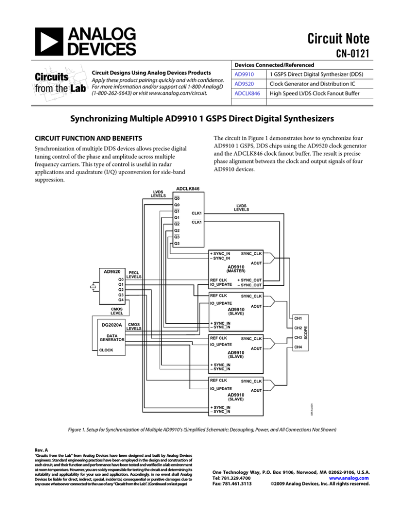
Circuit Note CN-0121 Devices Connected/Referenced Circuit Designs Using Analog Devices Products Apply these product pairings quickly and with confidence. For more information and/or support call 1-800-AnalogD (1-800-262-5643) or visit www.analog.com/circuit. AD9910 1 GSPS Direct Digital Synthesizer (DDS) AD9520 Clock Generator and Distribution IC ADCLK846 High Speed LVDS Clock Fanout Buffer Synchronizing Multiple AD9910 1 GSPS Direct Digital Synthesizers CIRCUIT FUNCTION AND BENEFITS The circuit in Figure 1 demonstrates how to synchronize four AD9910 1 GSPS, DDS chips using the AD9520 clock generator and the ADCLK846 clock fanout buffer. The result is precise phase alignment between the clock and output signals of four AD9910 devices. Synchronization of multiple DDS devices allows precise digital tuning control of the phase and amplitude across multiple frequency carriers. This type of control is useful in radar applications and quadrature (I/Q) upconversion for side-band suppression. LVDS LEVELS ADCLK846 Q0 Q0 Q1 LVDS LEVELS CLK1 Q1 Q2 CLK1 Q2 Q3 Q3 + SYNC_IN – SYNC_IN SYNC_CLK AD9910 AD9520 Q0 Q1 Q2 Q3 Q4 PECL LEVELS AOUT (MASTER) REF CLK IO_UPDATE REF CLK + SYNC_OUT – SYNC_OUT SYNC_CLK IO_UPDATE AD9910 CMOS LEVEL AOUT (SLAVE) CMOS LEVELS DATA GENERATOR + SYNC_IN – SYNC_IN REF CLK CH2 SYNC_CLK CH3 AOUT CH4 IO_UPDATE CLOCK SCOPE CH1 DG2020A AD9910 (SLAVE) + SYNC_IN – SYNC_IN REF CLK SYNC_CLK IO_UPDATE AOUT AD9910 + SYNC_IN – SYNC_IN 08514-001 (SLAVE) Figure 1. Setup for Synchronization of Multiple AD9910’s (Simplified Schematic: Decoupling, Power, and All Connections Not Shown) Rev. A “Circuits from the Lab” from Analog Devices have been designed and built by Analog Devices engineers. Standard engineering practices have been employed in the design and construction of each circuit, and their function and performance have been tested and verified in a lab environment at room temperature. However, you are solely responsible for testing the circuit and determining its suitability and applicability for your use and application. Accordingly, in no event shall Analog Devices be liable for direct, indirect, special, incidental, consequential or punitive damages due to any cause whatsoever connected to the use of any“Circuit from the Lab”. (Continued on last page) One Technology Way, P.O. Box 9106, Norwood, MA 02062-9106, U.S.A. Tel: 781.329.4700 www.analog.com Fax: 781.461.3113 ©2009 Analog Devices, Inc. All rights reserved. CN-0121 Circuit Note CIRCUIT DESCRIPTION The circuit in Figure 1 was constructed by connecting the respective evaluation boards for the individual products. Connections were made with matched cable lengths. The first of three basic requirements to synchronize multiple AD9910’s is to provide a co-incident reference clock (REF CLK). The setup uses the AD9520 as the REF CLK source for each AD9910 DDS. The AD9520 runs off an external crystal and the internal PLL. The AD9520 distributes phase aligned 1 GHz REF CLKs (PECL outputs) to all four AD9910 evaluation boards. It also provides a CMOS output clock to the Tektronix DG2020A data pattern generator for the IO_UPDATE. The next step for synchronization is to align the rising edge of SYNC_CLK for all four AD9910’s. The SYNC_CLK provides the reference for a co-incident IO_UPDATE. SYNC_CLK alignment is accomplished using the internal synchronization capability of the AD9910. The ADCLK846 distributes phase aligned SYNC_INs to all four AD9910s. See the AD9910 data sheet for more details on synchronization capability. The last requirement to synchronize multiple DDS devices is a co-incident IO_UPDATE. The IO_UPDATE must meet setup and hold times to SYNC_CLK. The IO_UPDATE shown in Figure 1 is sent synchronously to the SYNC_CLK. The last requirement now enables the DDS outputs to be controlled. Figures 4 and 5 show the DDS outputs in phase alignment. Having the devices synchronized to one another now enables predictable phase and/or amplitude adjustment between DDSs. Note, in Figure 5 the system clock was reduced to 100 MHz operation, and the outputs were unfiltered to display each DDS raw output. Figure 5 also shows the value of synchronization with each device outputting the same signal. To phase align the SYNC_CLK rising edges, one AD9910 is programmed as the master device and the others as slave devices. The SYNC_OUT of the master device is an LVDS signal buffered and distributed by the ADCLK846 to all AD9910 evaluation boards. The SYNC_IN signal (LVDS) must meet internal setup and hold time requirements of each device’s system clock. To help support this timing requirement, the AD9910 features the ability to delay the SYNC_OUT of the master. For further flexibility, the internal SYNC_IN path of each device can be independently delayed. C3 FREQUENCY 249.54MHz LOW SIGNAL AMPLITUDE 1 2 3 4 08514-003 Figure 2 shows all four SYNC_CLKs with the AD9910 internal synchronization circuit disabled. Note that the SYNC_CLKs are not inherently aligned even when the REF CLKs are phase aligned. CH1 1.00VΩ CH2 1.00VΩ CH3 1.00VΩ CH4 1.00VΩ M2.00ns CH1 480mV Figure 3. SYNC_CLK Are Aligned. C3 FREQUENCY 125.321MHz C3 FREQUENCY 250.76MHz LOW SIGNAL AMPLITUDE 1 In the setup of Figure 1, connections between boards were made using matched cables, making it possible to use the internal default delay values to phase align the SYNC_CLKs. Figure 3 shows SYNC_CLK phase alignment via the using the synchronization procedure described. 1 2 2 3 3 08514-002 4 CH1 1.00VΩ CH2 1.00VΩ CH3 1.00VΩ CH4 1.00VΩ M2.00ns CH2 480mV Figure 2. SYNC_CLKs Are Not Aligned. 08514-004 4 CH1 200mVΩ CH3 200mVΩ B W B W CH2 200mVΩ BW M5.00ns CH4 200mVΩ BW CH2 –80V Figure 4. Filtered DDS Outputs Phase Aligned Using the Setup in Figure 1. Rev. A | Page 2 of 3 Circuit Note CN-0121 LEARN MORE 1 AN-823 Application Note, Direct Digital Synthesizers in Clocking Applications. Analog Devices. 2 AN-837 Application Note, DDS-Based Clock Jitter Performance vs. DAC Reconstruction Filter Performance. Analog Devices. Kester, Walt. 2005. The Data Conversion Handbook. Analog Devices. Chapters 6 and 7. 3 Kester, Walt. 2006. High Speed System Applications. Analog Devices. Chapter 2, “Optimizing Data Converter Interfaces.” 4 08514-005 Kester, Walt. 2006. High Speed System Applications. Analog Devices. Chapter 3, “DACs, DDSs, PLLs, and Clock Distribution.” CH1 200mVΩ CH3 200mVΩ CH2 200mVΩ M20.0ns CH4 200mVΩ CH2 –80V Figure 5. DDS Unfiltered Outputs Phase Aligned Using the Setup in Figure 1. COMMON VARIATIONS Analog Devices offers a variety of direct digital synthesizers, clock distribution chips, and clock buffers to build a DDS-based clock generator. Refer to www.analog.com/dds and www.analog.com/clock for more information. MT-031 Tutorial, Grounding Data Converters and Solving the Mystery of AGND and DGND. Analog Devices. MT-085 Tutorial, Fundamentals of Direct Digital Synthesis (DDS), Analog Devices. MT-086 Tutorial, Fundamentals of Phase Locked Loops (PLL), Analog Devices. MT-101 Tutorial, Decoupling Techniques. Analog Devices. Data Sheets and Evaluation Boards AD9910 Data Sheet. AD9910 Evaluation Board. AD9520 Data Sheet. AD9520 Evaluation Board. ADCLK846 Data Sheet. ADCLK846 Evaluation Board. REVISION HISTORY 12/09—Rev. 0 to Rev. A Changes to Figure 1 .......................................................................... 1 10/09—Revision 0: Initial Version (Continued from first page) "Circuits from the Lab" are intended only for use with Analog Devices products and are the intellectual property of Analog Devices or its licensors. While you may use the "Circuits from the Lab" in the design of your product, no other license is granted by implication or otherwise under any patents or other intellectual property by application or use of the "Circuits from the Lab". Information furnished by Analog Devices is believed to be accurate and reliable. However, "Circuits from the Lab" are supplied "as is" and without warranties of any kind, express, implied, or statutory including, but not limited to, any implied warranty of merchantability, noninfringement or fitness for a particular purpose and no responsibility is assumed by Analog Devices for their use, nor for any infringements of patents or other rights of third parties that may result from their use. Analog Devices reserves the right to change any "Circuits from the Lab" at any time without notice, but is under no obligation to do so. Trademarks and registered trademarks are the property of their respective owners. ©2009 Analog Devices, Inc. All rights reserved. Trademarks and registered trademarks are the property of their respective owners. CN08514-0-12/09(A) Rev. A | Page 3 of 3


