Ethernet Clock Generator, 10 Clock Outputs AD9571 FEATURES
advertisement
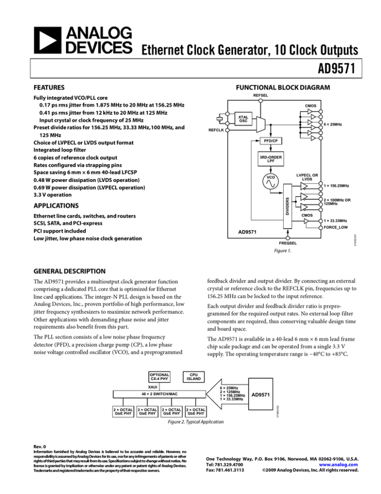
Ethernet Clock Generator, 10 Clock Outputs AD9571 FEATURES FUNCTIONAL BLOCK DIAGRAM REFSEL Fully integrated VCO/PLL core 0.17 ps rms jitter from 1.875 MHz to 20 MHz at 156.25 MHz 0.41 ps rms jitter from 12 kHz to 20 MHz at 125 MHz Input crystal or clock frequency of 25 MHz Preset divide ratios for 156.25 MHz, 33.33 MHz,100 MHz, and 125 MHz Choice of LVPECL or LVDS output format Integrated loop filter 6 copies of reference clock output Rates configured via strapping pins Space saving 6 mm × 6 mm 40-lead LFCSP 0.48 W power dissipation (LVDS operation) 0.69 W power dissipation (LVPECL operation) 3.3 V operation CMOS XTAL OSC 6 × 25MHz REFCLK PFD/CP 3RD-ORDER LPF LVPECL OR LVDS VCO DIVIDERS 1 × 156.25MHz APPLICATIONS Ethernet line cards, switches, and routers SCSI, SATA, and PCI-express PCI support included Low jitter, low phase noise clock generation 2 × 100MHz OR 125MHz CMOS 1 × 33.33MHz FREQSEL 07499-001 FORCE_LOW AD9571 Figure 1. GENERAL DESCRIPTION The AD9571 provides a multioutput clock generator function comprising a dedicated PLL core that is optimized for Ethernet line card applications. The integer-N PLL design is based on the Analog Devices, Inc., proven portfolio of high performance, low jitter frequency synthesizers to maximize network performance. Other applications with demanding phase noise and jitter requirements also benefit from this part. feedback divider and output divider. By connecting an external crystal or reference clock to the REFCLK pin, frequencies up to 156.25 MHz can be locked to the input reference. The PLL section consists of a low noise phase frequency detector (PFD), a precision charge pump (CP), a low phase noise voltage controlled oscillator (VCO), and a preprogrammed The AD9571 is available in a 40-lead 6 mm × 6 mm lead frame chip scale package and can be operated from a single 3.3 V supply. The operating temperature range is −40°C to +85°C. Each output divider and feedback divider ratio is preprogrammed for the required output rates. No external loop filter components are required, thus conserving valuable design time and board space. OPTIONAL CX-4 PHY CPU ISLAND XAUI 2 × OCTAL GbE PHY 2 × OCTAL GbE PHY 2 × OCTAL GbE PHY AD9571 07499-002 6 × 25MHz 2 × 125MHz 1 × 156.25MHz 1 × 33.33MHz 48 + 2 SWITCH/MAC 2 × OCTAL GbE PHY Figure 2. Typical Application Rev. 0 Information furnished by Analog Devices is believed to be accurate and reliable. However, no responsibility is assumed by Analog Devices for its use, nor for any infringements of patents or other rights of third parties that may result from its use. Specifications subject to change without notice. No license is granted by implication or otherwise under any patent or patent rights of Analog Devices. Trademarks and registeredtrademarks are the property of their respective owners. One Technology Way, P.O. Box 9106, Norwood, MA 02062-9106, U.S.A. www.analog.com Tel: 781.329.4700 Fax: 781.461.3113 ©2009 Analog Devices, Inc. All rights reserved. AD9571 TABLE OF CONTENTS Features .............................................................................................. 1 ESD Caution...................................................................................9 Applications ....................................................................................... 1 Pin Configuration and Function Descriptions ............................10 Functional Block Diagram .............................................................. 1 Typical Performance Characteristics ............................................12 General Description ......................................................................... 1 Terminology .....................................................................................13 Revision History ............................................................................... 2 Theory of Operation .......................................................................14 Specifications ..................................................................................... 3 Outputs .........................................................................................14 PLL Characteristics ...................................................................... 3 Phase Frequency Detector (PFD) and Charge Pump.............15 LVDS Clock Output Jitter............................................................ 4 Power Supply................................................................................15 LVPECL Clock Output Jitter....................................................... 5 CMOS Clock Distribution .........................................................15 CMOS Clock Output Jitter .......................................................... 5 LVPECL Clock Distribution ......................................................16 Reference Input ............................................................................. 5 LVDS Clock Distribution ...........................................................16 Clock Outputs ............................................................................... 6 Reference Input............................................................................16 Timing Characteristics................................................................. 6 Control Pins .................................................................................. 7 Power and Grounding Considerations and Power Supply Rejection .......................................................................................16 Power .............................................................................................. 7 Outline Dimensions ........................................................................17 Crystal Oscillator .......................................................................... 7 Ordering Guide............................................................................17 Timing Diagrams.......................................................................... 8 Absolute Maximum Ratings ............................................................ 9 Thermal Resistance ...................................................................... 9 REVISION HISTORY 8/09—Revision 0: Initial Version Rev. 0 | Page 2 of 20 AD9571 SPECIFICATIONS PLL CHARACTERISTICS Typical (typ) is given for VS = 3.3 V, TA = 25°C, unless otherwise noted. Table 1. Parameter PHASE NOISE CHARACTERISTICS PLL Noise (156.25 MHz LVDS Output) @ 1 kHz @ 10 kHz @ 100 kHz @ 1 MHz @ 10 MHz @ 30 MHz PLL Noise (125 MHz LVDS Output) @ 1 kHz @ 10 kHz @ 100 kHz @ 1 MHz @ 10 MHz @ 30 MHz PLL Noise (100 MHz LVDS Output) @ 1 kHz @ 10 kHz @ 100 kHz @ 1 MHz @ 10 MHz @ 30 MHz PLL Noise (156.25 MHz LVPECL Output) @ 1 kHz @ 10 kHz @ 100 kHz @ 1 MHz @ 10 MHz @ 30 MHz Min Typ Max Unit Test Conditions/Comments −120 −126 −126 −145 −151 −152 dBc/Hz dBc/Hz dBc/Hz dBc/Hz dBc/Hz dBc/Hz 33.33 MHz output disabled 33.33 MHz output disabled 33.33 MHz output disabled 33.33 MHz output disabled 33.33 MHz output disabled 33.33 MHz output disabled −122 −128 −128 −147 −152 −152 dBc/Hz dBc/Hz dBc/Hz dBc/Hz dBc/Hz dBc/Hz 33.33 MHz output disabled 33.33 MHz output disabled 33.33 MHz output disabled 33.33 MHz output disabled 33.33 MHz output disabled 33.33 MHz output disabled −122 −129 −129 −147 −150 −150 dBc/Hz dBc/Hz dBc/Hz dBc/Hz dBc/Hz dBc/Hz 33.33 MHz output disabled 33.33 MHz output disabled 33.33 MHz output disabled 33.33 MHz output disabled 33.33 MHz output disabled 33.33 MHz output disabled −120 −125 −125 −145 −151 −152 dBc/Hz dBc/Hz dBc/Hz dBc/Hz dBc/Hz dBc/Hz 33.33 MHz output disabled 33.33 MHz output disabled 33.33 MHz output disabled 33.33 MHz output disabled 33.33 MHz output disabled 33.33 MHz output disabled Rev. 0 | Page 3 of 20 AD9571 Parameter PLL Noise (125 MHz LVPECL Output) @ 1 kHz @ 10 kHz @ 100 kHz @ 1 MHz @ 10 MHz @ 30 MHz PLL Noise (100 MHz LVPECL Output) @ 1 kHz @ 10 kHz @ 100 kHz @ 1 MHz @ 10 MHz @ 30 MHz Phase Noise (33.33 MHz CMOS Output) @ 1 kHz @ 10 kHz @ 100 kHz @ 1 MHz @ 5 MHz Phase Noise (25 MHz CMOS Output) @ 1 kHz @ 10 kHz @ 100 kHz @ 1 MHz @ 5 MHz Spurious Content1 PLL Figures of Merit 1 Min Typ Max Unit Test Conditions/Comments −121 −127 −128 −148 −152 −153 dBc/Hz dBc/Hz dBc/Hz dBc/Hz dBc/Hz dBc/Hz 33.33 MHz output disabled 33.33 MHz output disabled 33.33 MHz output disabled 33.33 MHz output disabled 33.33 MHz output disabled 33.33 MHz output disabled −115 −121 −128 −148 −150 −150 dBc/Hz dBc/Hz dBc/Hz dBc/Hz dBc/Hz dBc/Hz 33.33 MHz output disabled 33.33 MHz output disabled 33.33 MHz output disabled 33.33 MHz output disabled 33.33 MHz output disabled 33.33 MHz output disabled −131 −138 −139 −151 −152 dBc/Hz dBc/Hz dBc/Hz dBc/Hz dBc/Hz −133 −143 −147 −148 −148 −70 −217.5 dBc/Hz dBc/Hz dBc/Hz dBc/Hz dBc/Hz dBc dBc/Hz Dominant amplitude with all outputs active When the 33.33 MHz, 100 MHz, and 125 MHz clocks are enabled simultaneously, a worst-case −50 dBc spurious content may be presented on Pin 21 and Pin 22 only. LVDS CLOCK OUTPUT JITTER Typical (typ) is given for VS = 3.3 V, TA = 25°C, unless otherwise noted. Table 2. Jitter Integration Bandwidth (Typ) 12 kHz to 20 MHz 100 MHz 0.50 125 MHz1, 33.33 MHz = Off/On 0.41/0.77 1.875 MHz to 20 MHz 200 kHz to 10 MHz 1 0.30 156.25 MHz 0.41 Unit ps rms 0.17 ps rms 0.24/0.66 ps rms The typical 125 MHz rms jitter data collected from the differential pair of Pin 21 and Pin 22, unless otherwise noted. Rev. 0 | Page 4 of 20 Test Conditions/Comments LVDS output frequency combinations are 1 × 156.25 MHz, 1 × 100 MHz, 1 × 125 MHz, 1 × 33.33 MHz LVDS output frequency combinations are 1 × 156.25 MHz, 1 × 100 MHz, 1 × 125 MHz, 1 × 33.33 MHz LVDS output frequency combinations are 1 × 156.25 MHz, 1 × 100 MHz, 1 × 125 MHz, 1 × 33.33 MHz AD9571 LVPECL CLOCK OUTPUT JITTER Typical (typ) is given for VS = 3.3 V, TA = 25°C, unless otherwise noted. Table 3. Jitter Integration Bandwidth (Typ) 12 kHz to 20 MHz 100 MHz 0.54 125 MHz1, 33.33 MHz = Off/On 0.42/2.0 1.875 MHz to 20 MHz 200 kHz to 10 MHz 1 0.31 156.25 MHz 0.45 Unit ps rms 0.22 ps rms 0.25/1.9 ps rms Test Conditions/Comments LVPECL output frequency combinations are 1 × 156.25 MHz, 1 × 100 MHz, 1 × 125 MHz, 1 × 33.33 MHz LVPECL output frequency combinations are 1 × 156.25 MHz, 1 × 100 MHz, 1 × 125 MHz, 1 × 33.33 MHz LVPECL output frequency combinations are 1 × 156.25 MHz, 1 × 100 MHz, 1 × 125 MHz, 1 × 33.33 MHz The typical 125 MHz rms jitter data collected from the differential pair of Pin 21 and Pin 22, unless otherwise noted. CMOS CLOCK OUTPUT JITTER Typical (typ) is given for VS = 3.3 V, TA = 25°C, unless otherwise noted. Table 4. Jitter Integration Bandwidth 12 kHz to 5 MHz 200 kHz to 5 MHz 25 MHz 0.82 0.80 33.33 MHz 0.53 0.43 Unit ps rms ps rms Test Conditions/Comments N/A N/A REFERENCE INPUT Typical (typ) is given for VS = 3.3 V ± 10%, TA = 25°C, unless otherwise noted. Minimum (min) and maximum (max) values are given over full VS and T A (−40°C to +85°C) variation. Table 5. Parameter CLOCK INPUT (REFCLK) Input Frequency Input High Voltage Input Low Voltage Input Current Input Capacitance Min Typ Max 25 2.0 0.8 +1.0 −1.0 2 Rev. 0 | Page 5 of 20 Unit MHz V V µA pF Test Conditions/Comments AD9571 CLOCK OUTPUTS Typical (typ) is given for VS = 3.3 V ± 10%, TA = 25°C, unless otherwise noted. Minimum (min) and maximum (max) values are given over full VS and T A (−40°C to +85°C) variation. Table 6. Parameter LVPECL CLOCK OUTPUTS Output Frequency Output High Voltage (VOH) Output Low Voltage (VOL) Output Differential Voltage (VOD) Duty Cycle LVDS CLOCK OUTPUTS Output Frequency Differential Output Voltage (VOD) Delta VOD Output Offset Voltage (VOS) Delta VOS Short-Circuit Current (ISA, ISB) Duty Cycle CMOS CLOCK OUTPUTS Output Frequency Output High Voltage (VOH) Output Low Voltage (VOL) Duty Cycle Min Typ Max Unit VS − 1.24 VS − 2.07 700 45 VS − 1.05 VS − 1.87 825 156.25 VS − 0.83 VS − 1.62 950 55 MHz V V mV % 250 350 1.125 1.25 156.25 475 25 1.375 25 24 55 MHz mV mV V mV mA % 33.33 MHz V V % 14 45 VS − 0.1 0.1 58 42 Test Conditions/Comments Output shorted to GND Sourcing 1.0 mA current Sinking 1.0 mA current TIMING CHARACTERISTICS Typical (typ) is given for VS = 3.3 V ± 10%, TA = 25°C, unless otherwise noted. Minimum (min) and maximum (max) values are given over full VS and T A (−40°C to +85°C) variation. Table 7. Parameter LVPECL Output Rise Time, tRP Output Fall Time, tFP LVDS Output Rise Time, tRL Output Fall Time, tFL CMOS Output Rise Time, tRC Output Fall Time, tFC Min Typ Max Unit 480 480 625 625 810 810 ps ps 160 160 350 350 540 540 ps ps 0.25 0.25 0.50 0.70 2.5 2.5 ns ns Rev. 0 | Page 6 of 20 Test Conditions/Comments Termination = 200 Ω to 0 V; CLOAD = 0 pF 20% to 80%, measured differentially 80% to 20%, measured differentially Termination = 100 Ω differential; CLOAD = 0 pF 20% to 80%, measured differentially 80% to 20%, measured differentially Termination = 50 Ω to 0 V; CLOAD = 5 pF 20% to 80% 80% to 20% AD9571 CONTROL PINS Typical (typ) is given for VS = 3.3 V ± 10%, TA = 25°C, unless otherwise noted. Minimum (min) and maximum (max) values are given over full VS and T A (−40°C to +85°C) variation. Table 8. Parameter INPUT CHARACTERISTICS REFSEL Pin Logic 1 Voltage Logic 0 Voltage Logic 1 Current Logic 0 Current FREQSEL Pin Logic 1 Voltage Logic 0 Voltage Logic 1 Current Logic 0 Current FORCE_LOW Pin Logic 1 Voltage Logic 0 Voltage Logic 1 Current Logic 0 Current Min Typ Max Unit 0.8 1.0 155 V V µA µA Test Conditions/Comments REFSEL has a 30 kΩ pull-up resistor. 2.0 FREQSEL has a 150 kΩ pull-up resistor and a 100 kΩ pull-down resistor. 2/3(VS) + 0.2 1/3(VS)-0.2 45 30 V V µA µA 0.8 240 2.0 V V µA µA FORCE_LOW has a 16 kΩ pull-down resistor. 2.0 POWER Typical (typ) is given for VS = 3.3 V ± 10%, TA = 25°C, unless otherwise noted. Minimum (min) and maximum (max) values are given over full VS and T A (−40°C to +85°C) variation. Table 9. Parameter Power Supply LVDS Power Dissipation LVPECL Power Dissipation Min 3.0 Typ 3.3 480 690 Max 3.6 600 860 Unit V mW mW Test Conditions/Comments CRYSTAL OSCILLATOR Typical (typ) is given for VS = 3.3 V ± 10%, TA = 25°C, unless otherwise noted. Minimum (min) and maximum (max) values are given over full VS and T A (−40°C to +85°C) variation. Table 10. Parameter CRYSTAL SPECIFICATION Frequency ESR Load Capacitance Phase Noise Stability Min Typ Max 25 50 14 −135 −30 +30 Rev. 0 | Page 7 of 20 Unit MHz Ω pF dBc/Hz ppm Test Conditions/Comments Fundamental mode @1 kHz offset AD9571 TIMING DIAGRAMS SINGLE-ENDED DIFFERENTIAL 80% 80% CMOS 5pF LOAD LVPECL tFP 07499-003 tRP tRC Figure 5. CMOS Timing, Single-Ended, 5 pF Load Figure 3. LVPECL Timing, Differential DIFFERENTIAL 80% LVDS tFL 07499-004 20% tRL tFC Figure 4. LVDS Timing, Differential Rev. 0 | Page 8 of 20 07499-005 20% 20% AD9571 ABSOLUTE MAXIMUM RATINGS Table 11. Parameter VS to GND REFCLK to GND BYPASSx to GND XO to GND FORCE_LOW, FREQSEL, and REFSEL to GND 25M, 33M, 100M/125M, and 156M to GND Junction Temperature1 Storage Temperature Range 1 THERMAL RESISTANCE θJA is specified for the worst-case conditions, that is, a device soldered in a circuit board for surface-mount packages. Thermal impedance measurements were taken on a 4-layer board in still air in accordance with EIA/JESD51-7. Rating −0.3 V to +3.6 V −0.3 V to VS + 0.3 V −0.3 V to VS + 0.3 V −0.3 V to VS + 0.3 V −0.3 V to VS + 0.3 V Table 12. Thermal Resistance Package Type 40-Lead LFCSP −0.3 V to VS + 0.3 V ESD CAUTION 150°C −65°C to +150°C See Table 12 for θJA. Stresses above those listed under Absolute Maximum Ratings may cause permanent damage to the device. This is a stress rating only; functional operation of the device at these or any other conditions above those indicated in the operational section of this specification is not implied. Exposure to absolute maximum rating conditions for extended periods may affect device reliability. Rev. 0 | Page 9 of 20 θJA 27.5 Unit °C/W AD9571 40 39 38 37 36 35 34 33 32 31 VS VS * FORCE_LOW BYPASS1 VS GND VS 25M 25M PIN CONFIGURATION AND FUNCTION DESCRIPTIONS PIN 1 INDICATOR AD9571 TOP VIEW (Not to Scale) LVPECL/ LVDS 30 29 28 27 26 25 24 23 22 21 25M 25M VS FREQSEL VS VS VS 33M 100M/125M 100M/125M NOTES 1. * = SHORT TO PIN 36. 2. ** = SHORT TO PIN 14. 3. NOTE THAT THE EXPOSED PADDLE ON THIS PACKAGE IS AN ELECTRICAL CONNECTION AS WELL AS A THERMAL ENHANCEMENT. FOR THE DEVICE TO FUNCTION PROPERLY, THE PADDLE MUST BE ATTACHED TO GROUND (GND). 07499-006 VS ** ** BYPASS2 VS VS 156M 156M 100M/125M 100M/125M 11 12 13 14 15 16 17 18 19 20 GND 1 VS 2 25M 3 25M 4 VS 5 XO 6 XO 7 REFCLK 8 REFSEL 9 GND 10 Figure 6. Pin Configuration 1 Table 13. Pin Function Descriptions Pin No. Mnemonic 2 VS 3, 4, 29, 30, 31, 32 25M 5 VS 6, 7 XO 8 REFCLK 9 REFSEL 11 VS 1, 10, 34 GND 14, 36 BYPASS2, BYPASS1 15 VS 16 VS 17 156M 18 156M 19, 21 100M/125M 20, 22 100M/125M 23 33M 24 VS 25 VS 26 VS 27 FREQSEL 28 VS Description Power Supply Connection for the 25M CMOS Buffer. CMOS 25 MHz Output. Power Supply Connection for the Crystal Oscillator. External 25 MHz Crystal. 25 MHz Reference Clock Input. Tie low when not in use. Logic Input. Used to select the reference source. Power Supply Connection for the GbE PLL. Ground Pins. The external paddle must be attached to GND. These pins are for bypassing each LDO to ground with a 220 nF capacitor. Power Supply Connection for the GbE VCO. Power Supply Connection for the 156M LVDS Output Buffer and Output Dividers. LVPECL/LVDS Output at 156.25 MHz. Complementary LVPECL/LVDS Output at 156.25 MHz. LVPECL/LVDS Output at 100 MHz or 125 MHz. Selected by FREQSEL pin strapping. Complementary LVPECL/LVDS Output at 100 MHz or 125 MHz. CMOS 33.33 MHz Output. Power Supply Connection for the 33M CMOS Output Buffer and Output Dividers. Power Supply Connection for the 100M/125M LVDS Output Buffer and Output Dividers. Power Supply Connection for the GbE PLL Feedback Divider. Logic Input. Used to configure output drivers. Power Supply Connection for the FC PLL Feedback Divider. Rev. 0 | Page 10 of 20 AD9571 Pin No. 33 35 37 39 40 1 Mnemonic VS VS FORCE_LOW VS VS Description Power Supply Connection for the 106.25 MHz LVDS Output Buffer and Output Dividers. Power Supply Connection for the FC VCO. Forces the 33.33 MHz output into a low state. Power Supply Connection for the FC PLL. Power Supply Connection for Miscellaneous Logic. The exposed paddle on this package is an electrical connection as well as a thermal enhancement. For the device to function properly, the paddle must be attached to ground (GND). Rev. 0 | Page 11 of 20 AD9571 TYPICAL PERFORMANCE CHARACTERISTICS –100 –100 –110 –110 PHASE NOISE (dBc/Hz) –120 –130 –140 –140 –150 10k 100k 1M 10M 100M FREQUENCY (Hz) –160 1k 07499-007 –160 1k –130 1M 10M 100M Figure 9. 156.25 MHz Phase Noise –100 –110 –110 PHASE NOISE (dBc/Hz) –100 –120 –130 –140 –150 –120 –130 –140 –150 10k 100k 1M FREQUENCY (Hz) 10M 100M 07499-008 PHASE NOISE (dBc/Hz) 100k FREQUENCY (Hz) Figure 7. 125 MHz Phase Noise –160 1k 10k 07499-009 –150 –120 Figure 8. 25 MHz Phase Noise –160 1k 10k 100k 1M FREQUENCY (Hz) Figure 10. 100 MHz Phase Noise Rev. 0 | Page 12 of 20 10M 100M 07499-010 PHASE NOISE (dBc/Hz) Both 100 MHz and 125 MHz outputs enabled; 33.33 MHz output disabled. AD9571 TERMINOLOGY Phase Jitter An ideal sine wave can be thought of as having a continuous and even progression of phase with time from 0 degrees to 360 degrees for each cycle. Actual signals, however, display a certain amount of variation from ideal phase progression over time. This phenomenon is called phase jitter. Although many causes can contribute to phase jitter, one major cause is random noise, which is characterized statistically as gaussian (normal) in distribution. This phase jitter leads to a spreading out of the energy of the sine wave in the frequency domain, producing a continuous power spectrum. This power spectrum is usually reported as a series of values whose units are dBc/Hz at a given offset in frequency from the sine wave (carrier). The value is a ratio (expressed in dB) of the power contained within a 1 Hz bandwidth with respect to the power at the carrier frequency. For each measurement, the offset from the carrier frequency is also given. Phase Noise When the total power contained within some interval of offset frequencies (for example, 12 kHz to 20 MHz) is integrated, it is called the integrated phase noise over that frequency offset interval, and it can be readily related to the time jitter due to the phase noise within that offset frequency interval. Phase noise has a detrimental effect on error rate performance by increasing eye closure at the transmitter output and reducing the jitter tolerance/sensitivity of the receiver. Time Jitter Phase noise is a frequency domain phenomenon. In the time domain, the same effect is exhibited as time jitter. When observing a sine wave, the time of successive zero crossings is seen to vary. In a square wave, the time jitter is seen as a displacement of the edges from their ideal (regular) times of occurrence. In both cases, the variations in timing from the ideal are the time jitter. Because these variations are random in nature, the time jitter is specified in units of seconds root mean square (rms) or 1 sigma of the gaussian distribution. Additive Phase Noise Additive phase noise is the amount of phase noise that is attributable to the device or subsystem being measured. The phase noise of any external oscillators or clock sources has been subtracted. This makes it possible to predict the degree to which the device impacts the total system phase noise when used in conjunction with the various oscillators and clock sources, each of which contributes its own phase noise to the total. In many cases, the phase noise of one element dominates the system phase noise. Additive Time Jitter Additive time jitter is the amount of time jitter that is attributable to the device or subsystem being measured. The time jitter of any external oscillators or clock sources has been subtracted. This makes it possible to predict the degree to which the device impacts the total system time jitter when used in conjunction with the various oscillators and clock sources, each of which contributes its own time jitter to the total. In many cases, the time jitter of the external oscillators and clock sources dominates the system time jitter. Rev. 0 | Page 13 of 20 AD9571 THEORY OF OPERATION REFSEL VS GND 25MHz 25M CMOS XTAL OSC 1 CMOS REFCLK 25M 25M 0 25M 25M CMOS PHASE FREQUENCY DETECTOR DIVIDE BY 25 VCO CHARGE PUMP 25M 156.25MHz 156M 156M DIVIDE BY 4 DIVIDE BY 4 LVPECL/ LVDS VLDO DIVIDE BY 4 DIVIDE BY 5 0 125MHz/ 100MHz 100M/125M 100M/125M 1 LVPECL/ LVDS LEVEL DECODE AD9571 DIVIDE BY 3 125MHz/ 100MHz 100M/125M 100M/125M 1 LVPECL/ LVDS 33.33MHz CMOS 33M 07499-011 DIVIDE BY 5 0 FREQSEL FORCE_LOW Figure 11. Detailed Block Diagram Figure 11 shows a block diagram of the AD9571. The chip consists of a PLL core, which is configured to generate the specific clock frequencies required for Ethernet applications, without any user programming. This PLL is based on proven Analog Devices synthesizer technology, noted for its exceptional phase noise performance. The AD9571 is highly integrated and includes loop filters, regulators for supply noise immunity, all the necessary dividers with multiple output buffers in a choice of formats, and a crystal oscillator. A user need only supply a 25 MHz reference clock or an external crystal to implement an entire line card clocking solution that does not require any processor intervention. Six copies of the 25 MHz reference source are also available. OUTPUTS Table 14 provides a summary of the outputs available. Table 14. Output Formats Frequency 25 MHz 156.25 MHz 100 MHz or 125 MHz 33.33 MHz Format CMOS LVPECL/LVDS LVPECL/LVDS CMOS Copies 6 1 2 1 Note that the pins labeled 100M/125M can provide 100 MHz or 125 MHz by strapping the FREQSEL pin as shown in Table 15. Rev. 0 | Page 14 of 20 AD9571 Table 15. FREQSEL Definition Frequency Available from Pin 19 and Pin 20 FREQSEL (MHZ) 0 125 1 100 NC 125 Frequency Available from Pin 21 and Pin 22 (MHZ) 125 100 100 PHASE FREQUENCY DETECTOR (PFD) AND CHARGE PUMP The PFD takes inputs from the reference clock and feedback divider to produce an output proportional to the phase and frequency difference between them. Figure 14 shows a simplified schematic. 3.3V CHARGE PUMP 3.5mA HIGH REFCLK D1 Q1 UP CLR1 OUT OUT 3.5mA HIGH Figure 12. LVDS Output Simplified Equivalent Circuit CLR2 DOWN D2 Q2 FEEDBACK DIVIDER The simplified equivalent circuits of the LVDS and LVPECL outputs are shown in Figure 12 and Figure 13. GND 07499-014 07499-012 CP Figure 14. PFD Simplified Schematic 3.3V POWER SUPPLY The AD9571 requires a 3.3 V ± 10% power supply for VS. The Specifications section gives the performance expected from the AD9571 with the power supply voltage within this range. The absolute maximum range of (−0.3 V) − (+3.6 V), with respect to GND, must never be exceeded on the VS pin. OUT GND 07499-013 OUT Figure 13. LVPECL Output Simplified Equivalent Circuit The differential outputs are factory programmed to either LVPECL or LVDS format, and either option can be sampled on request. CMOS drivers tend to generate more noise than differential outputs and, as a result, the proximity of the 33.33 MHz output to Pin 21 and Pin 22 does affect the jitter performance when FREQSEL = 0 (that is, when the differential output is generating 125 MHz). For this reason, the 33.33 MHz pin can be forced to a low state by asserting the FORCE_LOW signal on Pin 37 (see Table 16). An internal pull-down enables the 33.33 MHz output if the pin is not connected. Table 16. FORCE_LOW (Pin 37) Definition FORCE_LOW 33.33 MHz Output (Pin 23) 0 or NC 33.33 MHz 1 0 MHz Good engineering practice should be followed in the layout of power supply traces and the ground plane of the PCB. Bypass the power supply on the PCB with adequate capacitance (>10 µF). Bypass the AD9571 with adequate capacitors (0.1 µF) at all power pins as close as possible to the part. The layout of the AD9571 evaluation board is a good example. The exposed metal paddle on the AD9571 package is an electrical connection, as well as a thermal enhancement. For the device to function properly, the paddle must be properly attached to ground (GND). The PCB acts as a heat sink for the AD9571; therefore, this GND connection should provide a good thermal path to a larger dissipation area, such as a ground plane on the PCB. CMOS CLOCK DISTRIBUTION The AD9571 provides seven CMOS clock outputs (six 25 MHz and one 33.33 MHz) that are dedicated CMOS levels. Whenever single-ended CMOS clocking is used, some of the following general guidelines should be followed. Point-to-point nets should be designed such that a driver has one receiver only on the net, if possible. This allows for simple termination schemes and minimizes ringing due to possible mismatched impedances on the net. Series termination at the source is generally required to provide transmission line matching and/or to reduce current transients at the driver. Rev. 0 | Page 15 of 20 AD9571 The value of the resistor is dependent on the board design and timing requirements (typically 10 Ω to 100 Ω is used). CMOS outputs are limited in terms of the capacitive load or trace length that they can drive. Typically, trace lengths less than 6 inches are recommended to preserve signal rise/fall times and signal integrity. 3.3V 200Ω 100Ω LVPECL 200Ω LVDS CLOCK DISTRIBUTION GND Figure 15. Series Termination of CMOS Output Termination at the far end of the PCB trace is a second option. The CMOS outputs of the AD9571 do not supply enough current to provide a full voltage swing with a low impedance resistive, far-end termination, as shown in Figure 16. The far-end termination network should match the PCB trace impedance and provide the desired switching point. The reduced signal swing may still meet receiver input requirements in some applications. This can be useful when driving long trace lengths on less critical nets. Low voltage differential signaling (LVDS) is a second differential output option for the AD9571. LVDS uses a current mode output stage with a factory programmed current level. The normal value (default) for this current is 3.5 mA, which yields a 350 mV output swing across a 100 Ω resistor. The LVDS outputs meet or exceed all ANSI/TIA/EIA-644 specifications. A recommended termination circuit for the LVDS outputs is shown in Figure 19. 50Ω 100Ω LVDS LVDS 50Ω 07499-019 5pF 07499-015 MICROSTRIP Figure 19. LVDS Output Termination VPULLUP = 3.3V See the AN-586 Application Note on the Analog Devices website at www.analog.com for more information about LVDS. 100Ω 50Ω DIFFERENTIAL (COUPLED) Figure 18. LVPECL with Parallel Transmission Line CMOS 10Ω 0.1nF 07499-018 LVPECL 60.4Ω 1.0 INCH 10Ω 3.3V 0.1nF CMOS REFERENCE INPUT 5pF 07499-016 100Ω The low voltage, positive emitter-coupled logic (LVPECL) outputs of the AD9571 provide the lowest jitter clock signals available from the AD9571. The LVPECL outputs (because they are open emitter) require a dc termination to bias the output transistors. The simplified equivalent circuit in Figure 13 shows the LVPECL output stage. By default, the crystal oscillator is enabled and used as the reference source, which requires the connection of an external 25 MHz crystal. The REFSEL pin is pulled high internally by about 30 kΩ to support default operation. When REFSEL is tied low, the crystal oscillator is powered down, and the REFCLK pin must provide a good quality 25 MHz reference clock instead. This single-ended input can be driven by either a dc-coupled LVCMOS level signal or an ac-coupled sine wave or square wave, provided that an external divider is used to bias the input at VS/2. In most applications, a standard LVPECL far-end termination is recommended, as shown in Figure 17. The resistor network is designed to match the transmission line impedance (50 Ω) and the desired switching threshold (1.3 V). Table 17. REFSEL Definition REFSEL Reference Source 0 REFCLK input 1 Internal crystal oscillator Figure 16. CMOS Output with Far-End Termination LVPECL CLOCK DISTRIBUTION 3.3V 3.3V 50Ω 127Ω SINGLE-ENDED (NOT COUPLED) POWER AND GROUNDING CONSIDERATIONS AND POWER SUPPLY REJECTION 3.3V LVPECL 50Ω VT = VCC – 1.3V 83Ω 83Ω Figure 17. LVPECL Far-End Termination 07499-017 LVPECL 127Ω Many applications seek high speed and performance under less than ideal operating conditions. In these application circuits, the implementation and construction of the PCB is as important as the circuit design. Proper RF techniques must be used for device selection, placement, and routing, as well as for power supply bypassing and grounding to ensure optimum performance. Rev. 0 | Page 16 of 20 AD9571 OUTLINE DIMENSIONS 0.30 0.25 0.18 31 40 30 0.50 BSC 1 TOP VIEW 0.80 0.75 0.70 4.70 SQ 4.50 10 11 20 0.05 MAX 0.02 NOM COPLANARITY 0.08 0.20 REF SEATING PLANE *4.80 EXPOSED PAD 21 0.45 0.40 0.35 PIN 1 INDICATOR BOTTOM VIEW 0.25 MIN FOR PROPER CONNECTION OF THE EXPOSED PAD, REFER TO THE PIN CONFIGURATION AND FUNCTION DESCRIPTIONS SECTION OF THIS DATA SHEET. COMPLIANT TO JEDEC STANDARDS MO-220-WJJD-5 WITH EXCEPTION TO EXPOSED PAD DIMENSION. 072709-A PIN 1 INDICATOR 6.10 6.00 SQ 5.90 Figure 20. 40-Lead Lead Frame Chip Scale Package [LFCSP_WQ] 6 mm × 6 mm Body, Very Very Thin Quad (CP-40-7) Dimensions shown in millimeters ORDERING GUIDE Model AD9571ACPZLVD1, 2 AD9571ACPZLVD-RL1, 2 Temperature Range −40°C to +85°C −40°C to +85°C AD9571ACPZLVD-R71, 2 −40°C to +85°C AD9571ACPZPEC1, 3 AD9571ACPZPEC-R71, 3 −40°C to +85°C −40°C to +85°C AD9571ACPZPEC-RL1, 3 −40°C to +85°C AD9571-EVALZ-LVD1, 2 AD9571-EVALZ-PEC1, 3 Package Description 40-Lead Lead Frame Chip Scale Package [LFCSP_WQ] 40-Lead Lead Frame Chip Scale Package [LFCSP_WQ], 7” Tape Reel, 2,500 Pieces 40-Lead Lead Frame Chip Scale Package [LFCSP_WQ], 7” Tape Reel, 750 Pieces 40-Lead Lead Frame Chip Scale Package [LFCSP_WQ] 40-Lead Lead Frame Chip Scale Package [LFCSP_WQ], 7” Tape Reel, 750 Pieces 40-Lead Lead Frame Chip Scale Package [LFCSP_WQ], 7” Tape Reel, 2,500 Pieces Evaluation Board Evaluation Board 1 Z = RoHS Compliant Part. LVD indicates LVDS compliant, differential clock outputs. 3 PEC indicates LVPECL compliant, differential clock outputs. 2 Rev. 0 | Page 17 of 20 Package Option CP-40-7 CP-40-7 CP-40-7 CP-40-7 CP-40-7 CP-40-7 AD9571 NOTES Rev. 0 | Page 18 of 20 AD9571 NOTES Rev. 0 | Page 19 of 20 AD9571 NOTES ©2009 Analog Devices, Inc. All rights reserved. Trademarks and registered trademarks are the property of their respective owners. D07499-0-8/09(0) Rev. 0 | Page 20 of 20

