Understanding How a Voltage Regulator Works General Design Fundamentals
advertisement

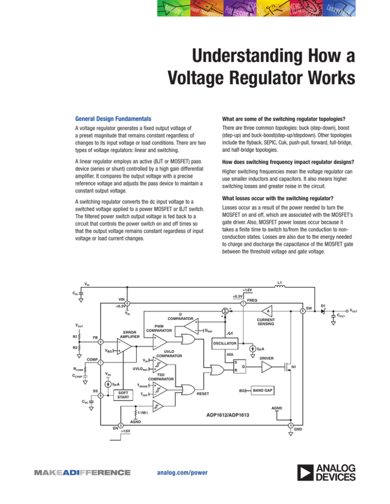
Understanding How a Voltage Regulator Works General Design Fundamentals What are some of the switching regulator topologies? A voltage regulator generates a fixed output voltage of a preset magnitude that remains constant regardless of changes to its input voltage or load conditions. There are two types of voltage regulators: linear and switching. There are three common topologies: buck (step-down), boost (step-up) and buck-boost(step-up/stepdown). Other topologies include the flyback, SEPIC, Cuk, push-pull, forward, full-bridge, and half-bridge topologies. A linear regulator employs an active (BJT or MOSFET) pass device (series or shunt) controlled by a high gain differential amplifier. It compares the output voltage with a precise reference voltage and adjusts the pass device to maintain a constant output voltage. How does switching frequency impact regulator designs? Higher switching frequencies mean the voltage regulator can use smaller inductors and capacitors. It also means higher switching losses and greater noise in the circuit. What losses occur with the switching regulator? A switching regulator converts the dc input voltage to a switched voltage applied to a power MOSFET or BJT switch. The filtered power switch output voltage is fed back to a circuit that controls the power switch on and off times so that the output voltage remains constant regardless of input voltage or load current changes. Losses occur as a result of the power needed to turn the MOSFET on and off, which are associated with the MOSFET’s gate driver. Also, MOSFET power losses occur because it takes a finite time to switch to/from the conduction to nonconduction states. Losses are also due to the energy needed to charge and discharge the capacitance of the MOSFET gate between the threshold voltage and gate voltage. L1 VIN >1.6V CIN <0.3V VIN <0.3V 6 7 VIN D COMPARATOR VOUT R1 PWM COMPARATOR ERROR AMPLIFIER FB VIN 1 RCOMP 8 CSS 5𝛍A S R DRIVER Q N1 TSD COMPARATOR 5𝛍A SS CURRENT SENSING UVLO COMPARATOR TSENSE SOFT START TREF RESET BG BAND GAP AGND 1.1MΩ EN 3 ADP1612/ADP1613 AGND 4 >1.6V analog.com/power SW D1 VOUT COUT DREF UVLOREF VSS CCOMP 5 OSCILLATOR VBG COMP A + 2 R2 FREQ + GND What are the usual applications for linear and switching regulators? What design specifications are important for a voltage regulator IC? The linear regulator’s power dissipation is directly proportional to its output current for a given input and output voltage, so typical efficiencies can be 50% or even lower. Using the optimum components, a switching regulator can achieve efficiencies in the 90% range. However, the noise output from a linear regulator is much lower than a switching regulator with the same output voltage and current requirements. Typically, the switching regulator can drive higher current loads than a linear regulator. Among the basic parameters are input voltage, output voltage, and output current. Depending on the application, other parameters may be important, such as output ripple voltage, load transient response, output noise, and efficiency. Important parameters for the linear regulator are dropout voltage, PSRR (power supply rejection ratio), and output noise. How does a switching regulator control its output? Switching regulators require a means to vary their output voltage in response to input and output voltage changes. One approach is to use PWM that controls the input to the associated power switch, which controls its on and off time (duty cycle). In operation, the regulator’s filtered output voltage is fed back to the PWM controller to control the duty cycle. If the filtered output tends to change, the feedback applied to the PWM controller varies the duty cycle to maintain a constant output voltage. Analog Devices, Inc. Worldwide Headquarters Analog Devices, Inc. One Technology Way P.O. Box 9106 Norwood, MA 02062-9106 U.S.A. Tel: 781.329.4700 (800.262.5643, U.S.A. only) Fax: 781.461.3113 Analog Devices, Inc. Europe Headquarters Analog Devices, Inc. Wilhelm-Wagenfeld-Str. 6 80807 Munich Germany Tel: 49.89.76903.0 Fax: 49.89.76903.157 Analog Devices, Inc. Japan Headquarters Analog Devices, KK New Pier Takeshiba South Tower Building 1-16-1 Kaigan, Minato-ku, Tokyo, 105-6891 Japan Tel: 813.5402.8200 Fax: 813.5402.1064 Analog Devices, Inc. Southeast Asia Headquarters Analog Devices 22/F One Corporate Avenue 222 Hu Bin Road Shanghai, 200021 China Tel: 86.21.2320.8000 Fax: 86.21.2320.8222 ©2009 Analog Devices, Inc. All rights reserved. Trademarks and registered trademarks are the property of their respective owners. T08503-0-8/09 analog.com/power


