Center (n) layer: donors. Donors donate electrons; with all... electrons, conduction is dominated by negative particles. n is for...
advertisement
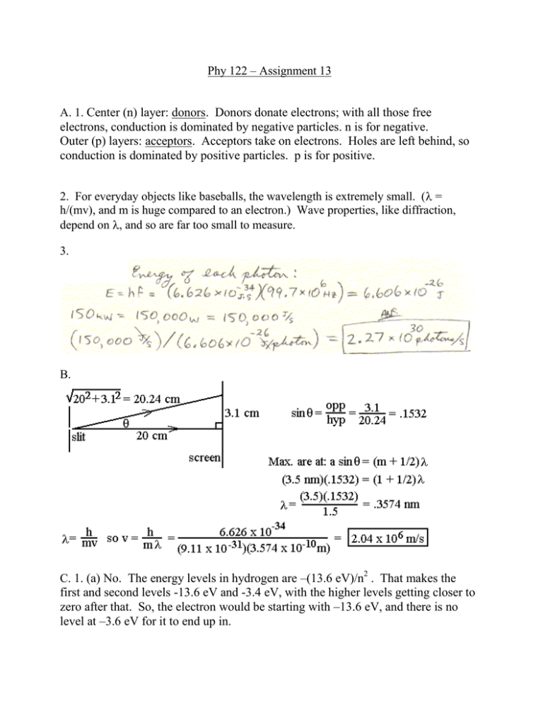
Phy 122 – Assignment 13 A. 1. Center (n) layer: donors. Donors donate electrons; with all those free electrons, conduction is dominated by negative particles. n is for negative. Outer (p) layers: acceptors. Acceptors take on electrons. Holes are left behind, so conduction is dominated by positive particles. p is for positive. 2. For everyday objects like baseballs, the wavelength is extremely small. ( = h/(mv), and m is huge compared to an electron.) Wave properties, like diffraction, depend on , and so are far too small to measure. 3. B. C. 1. (a) No. The energy levels in hydrogen are –(13.6 eV)/n2 . That makes the first and second levels -13.6 eV and -3.4 eV, with the higher levels getting closer to zero after that. So, the electron would be starting with –13.6 eV, and there is no level at –3.6 eV for it to end up in. (b) Yes. This would get the electron up to +.4 eV. An energy of zero or more knocks the electron right out of the atom. The energy of a free electron is not quantized, so +.4 eV works just fine. 2. D. 1. The energy gap equals the energy of the emitted photon: E = hf where f = c/ . 2. Charge may or may not build up in the center layer, depending on whether it is drained off by the small current Ib. (The top picture shows holes getting stuck in the n layer of a pnp.) This layer of charge repels additional charge trying to flow toward it, shutting off the current. If it’s not there, the current flows. 3. Note that it asks for the wavelength of the electron, not the wavelength of the light it gives off if it jumps to another level.(A common mistake.) For constructive interference, the circumference of the electron’s orbit must be a whole number of wavelengths: 2πr = nλ. (B should actually be exactly double A, but number rounding made them a little off.) E. . 1. Connecting the battery one way sucks free charges out of the junction, making it like an insulator. (No current due to lack of anything free to flow.) The other way dumps lots of free charges in, for the opposite effect. 2. To be absorbed by a semiconductor, a photon must make electron jump across the gap from the valence band. That the photon’s energy must be at least as much as the size of gap, or there won’t be an allowed energy for it to land in. an means the So, when the electron in the H atom falls from 4 to 2, or 5 to 2, or …, CdS can absorb the resulting photon. But, the 3 to 2 line has too little energy to get CdS’s electrons across the gap, so those photons pass through the crystal instead. (It’s transparent to that color, but opaque to the others.) F. 1. a. - 90° through +90°. (-90° if the circuit is purely capacitive, +90° if purely inductive. Various mixtures of C, L and R can give you any angle in between.) b. 0° If XL = XC, the opposite side of this triangle has a length of zero, making the phase angle zero. 2.
