16-Bit, 1 MSPS PulSAR ADC in MSOP AD7980-EP Enhanced Product FEATURES
advertisement
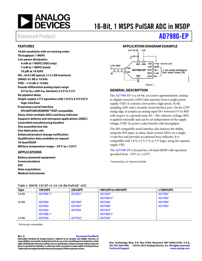
16-Bit, 1 MSPS PulSAR ADC in MSOP AD7980-EP Enhanced Product APPLICATION DIAGRAM EXAMPLE 16-bit resolution with no missing codes Throughput: 1 MSPS Low power dissipation 4 mW at 1 MSPS (VDD only) 7 mW at 1 MSPS (total) 70 μW at 10 kSPS INL: ±0.6 LSB typical, ±1.5 LSB maximum SINAD: 91 dB @ 10 kHz THD: −114 dB @ 10 kHz Pseudo differential analog input range 0 V to VREF with VREF between 2.5 V to 5.5 V No pipeline delay Single-supply 2.5 V operation with 1.8 V/2.5 V/3 V/5 V logic interface Proprietary serial interface SPI/QSPI/MICROWIRE™/DSP compatible Daisy-chain multiple ADCs and busy indicator Supports defense and aerospace applications (AQEC) Controlled manufacturing baseline One assembly/test site One fabrication site Enhanced product change notification Qualification data available on request 10-lead MSOP Military temperature range: −55°C to +125°C 2.5V TO 5V 2.5V VIO REF VDD 0 TO VREF IN+ IN– 1.8V TO 5.0V SDI AD7980-EP SCK SDO GND 3- OR 4-WIRE INTERFACE (SPI, DAISY CHAIN, CS) CNV 09304-001 FEATURES Figure 1. GENERAL DESCRIPTION The AD7980-EP1 is a 16-bit, successive approximation, analogto-digital converter (ADC) that operates from a single power supply, VDD. It contains a low power, high speed, 16-bit sampling ADC and a versatile serial interface port. On the CNV rising edge, it samples an analog input IN+ between 0 V to REF with respect to a ground sense IN−. The reference voltage, REF, is applied externally and can be set independent of the supply voltage, VDD. Its power scales linearly with throughput. The SPI-compatible serial interface also features the ability, using the SDI input, to daisy-chain several ADCs on a single, 3-wire bus and provides an optional busy indicator. It is compatible with 1.8 V, 2.5 V, 3 V, or 5 V logic, using the separate supply VIO. The AD7980-EP is housed in a 10-lead MSOP with operation specified from −55°C to +125°C. APPLICATIONS Battery-powered equipment Communications ATE Data acquisitions Medical instruments 1 Protected by U.S. Patent 6,703,961. Table 1. MSOP, LFCSP 14-/16-/18-Bit PulSAR® ADC Type 18-Bit 100 kSPS AD7989-11 250 kSPS AD76911 16-Bit AD7680 AD7683 AD7684 AD7988-11 AD7940 AD76851 AD76871 AD7694 14-Bit 1 AD79421 400 kSPS to 500 kSPS AD76901 AD7989-51 AD76861 AD76881 AD76931 AD7988-51 AD79461 ≥1000 kSPS AD79821 AD79841 AD79801 AD79831 Pin-for-pin compatible. Rev. A Document Feedback Information furnished by Analog Devices is believed to be accurate and reliable. However, no responsibility is assumed by Analog Devices for its use, nor for any infringements of patents or other rights of third parties that may result from its use. Specifications subject to change without notice. No license is granted by implication or otherwise under any patent or patent rights of Analog Devices. Trademarks and registered trademarks are the property of their respective owners. One Technology Way, P.O. Box 9106, Norwood, MA 02062-9106, U.S.A. Tel: 781.329.4700 ©2010–2015 Analog Devices, Inc. All rights reserved. Technical Support www.analog.com AD7980-EP Enhanced Product TABLE OF CONTENTS Features .............................................................................................. 1 Absolute Maximum Ratings ............................................................6 Applications ....................................................................................... 1 ESD Caution...................................................................................6 Application Diagram Example........................................................ 1 Pin Configurations and Function Descriptions ............................7 General Description ......................................................................... 1 Typical Performance Characteristics ..............................................8 Revision History ............................................................................... 2 Outline Dimensions ....................................................................... 12 Specifications..................................................................................... 3 Ordering Guide .......................................................................... 12 Timing Specifications....................................................................... 5 REVISION HISTORY 7/15—Rev. 0 to Rev. A Changes to Product Title, Features Section, and Table 1 ............ 1 Added Patent Note, Note 1 .............................................................. 1 Changes to Table 2 ............................................................................ 3 Changes to Table 3 ............................................................................ 4 Changes to Table 6 ............................................................................ 7 Changes to Figure 11, Figure 12, Figure 14, Figure 15 ................ 9 Changes to Figure 17, Figure 20, Figure 21 ................................. 10 Changes to Ordering Guide .......................................................... 12 9/10—Revision 0: Initial Version Rev. A | Page 2 of 12 Enhanced Product AD7980-EP SPECIFICATIONS VDD = 2.5 V, VIO = 2.3 V to 5.5 V, VREF = 5 V, TA = –55°C to +125°C, unless otherwise noted. Table 2. Parameter RESOLUTION ANALOG INPUT Voltage Range Absolute Input Voltage Analog Input CMRR Leakage Current @ 25°C ACCURACY No Missing Codes Differential Linearity Error Integral Linearity Error Transition Noise Gain Error, TMIN to TMAX2 Gain Error Temperature Drift Zero Error, TMIN to TMAX2 Zero Temperature Drift Power Supply Sensitivity THROUGHPUT Conversion Rate Transient Response AC ACCURACY Dynamic Range Oversampled Dynamic Range Signal-to-Noise Ratio, SNR Spurious-Free Dynamic Range, SFDR Total Harmonic Distortion, THD Signal-to-(Noise + Distortion), SINAD Conditions Min 16 IN+ − IN− IN+ IN− fIN = 100 kHz Acquisition phase 0 −0.1 −0.1 Typ Max VREF VREF + 0.1 +0.1 60 1 16 −0.9 REF = 5 V REF = 2.5 V REF = 5 V REF = 2.5 V REF = 5 V REF = 2.5 V −1.5 −0.62 VDD = 2.5 V ± 5% VIO ≥ 2.3 V up to 85°C, VIO ≥ 3.3 V above 85°C up to 125°C Full-scale step ±0.4 ±0.55 ±0.6 ±0.65 0.6 1.0 ±2 ±0.35 ±0.08 0.54 ±0.1 0 VREF = 5 V VREF = 2.5 V fO = 10 kSPS fIN = 10 kHz, VREF = 5 V fIN = 10 kHz, VREF = 2.5 V fIN = 10 kHz fIN = 10 kHz fIN = 10 kHz, VREF = 5 V fIN = 10 kHz, VREF = 2.5 V +0.9 +1.5 +0.62 2 Rev. A | Page 3 of 12 V V V dB nA Bits LSB1 LSB1 LSB1 LSB1 LSB1 LSB1 LSB1 ppm/°C mV ppm/°C LSB1 1 MSPS 290 ns 92 87 111 91.5 87 −110 −114 91 86.5 LSB means least significant bit. With the 5 V input range, 1 LSB is 76.3 µV. These specifications include full temperature range variation, but not the error contribution from the external reference. 3 All specifications in dB are referred to a full-scale input FSR. Tested with an input signal at 0.5 dB below full scale, unless otherwise specified. 1 Unit Bits dB3 dB3 dB3 dB3 dB3 dB3 dB3 dB3 dB3 AD7980-EP Enhanced Product VDD = 2.5 V, VIO = 2.3 V to 5.5 V, VREF = 5 V, TA = –55°C to +125°C, unless otherwise noted. Table 3. Parameter REFERENCE Voltage Range Load Current SAMPLING DYNAMICS −3 dB Input Bandwidth Aperture Delay DIGITAL INPUTS Logic Levels VIL VIH VIL VIH IIL IIH DIGITAL OUTPUTS Data Format Pipeline Delay VOL VOH POWER SUPPLIES VDD VIO VIO Range Standby Current1, 2 Power Dissipation Total VDD Only REF Only VIO Only Energy per Conversion TEMPERATURE RANGE Specified Performance 1 2 Conditions Min Typ 2.4 Max Unit 5.1 1 MSPS, REF = 5 V 330 V µA VDD = 2.5 V 10 2.0 MHz ns VIO > 3V VIO > 3V VIO ≤ 3V VIO ≤ 3V –0.3 0.7 × VIO –0.3 0.9 × VIO −1 −1 Serial 16 bits straight binary Conversion results available immediately after completed conversion 0.4 VIO − 0.3 ISINK = 500 µA ISOURCE = −500 µA 2.375 2.3 1.8 Specified performance VDD and VIO = 2.5 V, 25°C VDD = 2.625 V, VREF = 5 V, VIO = 3 V 10 kSPS throughput 1 MSPS throughput TMIN to TMAX 0.3 × VIO VIO + 0.3 0.1 × VIO VIO + 0.3 +1 +1 2.5 2.625 5.5 5.5 0.35 70 7.0 4 1.7 1.3 7.0 −55 With all digital inputs forced to VIO or GND as required. During the acquisition phase. Rev. A | Page 4 of 12 10 +125 V V µA µA µA V V V V V μA µW mW mW mW mW nJ/sample °C Enhanced Product AD7980-EP TIMING SPECIFICATIONS −55°C to +125°C, VDD = 2.37 V to 2.63 V, VIO = 3.3 V to 5.5 V, unless otherwise stated. See Figure 2 and Figure 3 for load conditions. Table 4. Parameter Conversion Time: CNV Rising Edge to Data Available Acquisition Time Time Between Conversions CNV Pulse Width (CS Mode) SCK Period (CS Mode) VIO Above 4.5 V VIO Above 3 V VIO Above 2.7 V VIO Above 2.3 V SCK Period (Chain Mode) VIO Above 4.5 V VIO Above 3 V VIO Above 2.7 V VIO Above 2.3 V SCK Low Time SCK High Time SCK Falling Edge to Data Remains Valid SCK Falling Edge to Data Valid Delay VIO Above 4.5 V VIO Above 3 V VIO Above 2.7 V VIO Above 2.3 V CNV or SDI Low to SDO D15 MSB Valid (CS Mode) VIO Above 3 V VIO Above 2.3 V CNV or SDI High or Last SCK Falling Edge to SDO High Impedance (CS Mode) SDI Valid Setup Time from CNV Rising Edge SDI Valid Hold Time from CNV Rising Edge (CS Mode) SDI Valid Hold Time from CNV Rising Edge (Chain Mode) SCK Valid Setup Time from CNV Rising Edge (Chain Mode) SCK Valid Hold Time from CNV Rising Edge (Chain Mode) SDI Valid Setup Time from SCK Falling Edge (Chain Mode) SDI Valid Hold Time from SCK Falling Edge (Chain Mode) SDI High to SDO High (Chain Mode with Busy Indicator) IOL IOH tSCKL tSCKH tHSDO tDSDO 9.5 11 12 14 ns ns ns ns 10 15 20 ns ns ns ns ns ns ns ns ns ns ns tEN tDIS tSSDICNV tHSDICNV tHSDICNV tSSCKCNV tHSCKCNV tSSDISCK tHSDISCK tDSDOSDI 5 2 0 5 5 2 3 15 Y% VIO1 tDELAY VIH2 VIL2 1FOR VIO ≤ 3.0V, X = 90 AND Y = 10; FOR VIO > 3.0V X = 70, AND Y = 30. 2MINIMUM V AND MAXIMUM V USED. SEE DIGITAL INPUTS IH IL 09304-002 500µA Unit ns ns ns ns ns ns ns ns ns ns ns ns ns ns ns ns ns 11.5 13 14 16 4.5 4.5 3 VIH2 VIL2 1.4V Max 710 tSCK X% VIO1 CL 20pF Typ 10.5 12 13 15 tDELAY TO SDO Min 500 290 1000 10 SPECIFICATIONS IN TABLE 3. Figure 2. Load Circuit for Digital Interface Timing Figure 3. Voltage Levels for Timing Rev. A | Page 5 of 12 09304-003 500µA Symbol tCONV tACQ tCYC tCNVH tSCK AD7980-EP Enhanced Product ABSOLUTE MAXIMUM RATINGS Table 5. Parameter Analog Inputs IN+, IN− to GND Supply Voltage REF, VIO to GND VDD to GND VDD to VIO Digital Inputs to GND Digital Outputs to GND Storage Temperature Range Junction Temperature θJA Thermal Impedance (10-Lead MSOP) θJC Thermal Impedance (10-Lead MSOP) Lead Temperature Vapor Phase (60 sec) Infrared (15 sec) Rating −0.3 V to VREF + 0.3 V or ±130 mA −0.3 V to +6 V −0.3 V to +3 V +3 V to −6 V −0.3 V to VIO + 0.3 V −0.3 V to VIO + 0.3 V −65°C to +150°C 150°C 200°C/W Stresses at or above those listed under Absolute Maximum Ratings may cause permanent damage to the product. This is a stress rating only; functional operation of the product at these or any other conditions above those indicated in the operational section of this specification is not implied. Operation beyond the maximum operating conditions for extended periods may affect product reliability. ESD CAUTION 44°C/W 215°C 220°C Rev. A | Page 6 of 12 Enhanced Product AD7980-EP REF 1 VDD 2 IN+ 3 IN– 4 GND 5 AD7980-EP TOP VIEW (Not to Scale) 10 VIO 9 SDI 8 SCK 7 SDO 6 CNV 09304-004 PIN CONFIGURATIONS AND FUNCTION DESCRIPTIONS Figure 4. 10-Lead MSOP Pin Configuration Table 6. Pin Function Descriptions Pin No. 1 Mnemonic REF Type1 AI 2 3 VDD IN+ P AI 4 5 6 IN− GND CNV AI P DI 7 8 9 SDO SCK SDI DO DI DI 10 VIO P Description Reference Input Voltage. The REF range is from 2.4 V to 5.1 V. It is referred to the GND pin. This pin should be decoupled closely to the pin with a 10 µF capacitor. Power Supply. Analog Input. It is referred to IN−. The voltage range, for example, the difference between IN+ and IN−, is 0 V to VREF. Analog Input Ground Sense. To be connected to the analog ground plane or to a remote sense ground. Power Supply Ground. Convert Input. This input has multiple functions. On its leading edge, it initiates the conversions and selects the interface mode of the part, chain, or CS mode. In CS mode, it enables the SDO pin when low. In chain mode, the data should be read when CNV is high. Serial Data Output. The conversion result is output on this pin. It is synchronized to SCK. Serial Data Clock Input. When the part is selected, the conversion result is shifted out by this clock. Serial Data Input. This input provides multiple features. It selects the interface mode of the ADC as follows. Chain mode is selected if SDI is low during the CNV rising edge. In this mode, SDI is used as a data input to daisy-chain the conversion results of two or more ADCs onto a single SDO line. The digital data level on SDI is output on SDO with a delay of 16 SCK cycles. CS mode is selected if SDI is high during the CNV rising edge. In this mode, either SDI or CNV can enable the serial output signals when low; if SDI or CNV is low when the conversion is complete, the busy indicator feature is enabled. Input/Output Interface Digital Power. Nominally at the same supply as the host interface (1.8 V, 2.5 V, 3 V, or 5 V). AI = analog input, DI = digital input, DO = digital output, and P = power. 1 Rev. A | Page 7 of 12 AD7980-EP Enhanced Product TYPICAL PERFORMANCE CHARACTERISTICS VDD = 2.5 V, VREF = 5.0 V, VIO = 3.3 V, unless otherwise noted. 1.25 1.00 POSITIVE INL: +0.33 LSB NEGATIVE INL: –0.39 LSB 1.00 POSITIVE INL: +0.18 LSB NEGATIVE INL: –0.21 LSB 0.75 0.75 0.50 0.25 DNL (LSB) INL (LSB) 0.50 0 –0.25 0.25 0 –0.25 –0.50 –0.50 –0.75 0 16384 32768 65536 49152 CODE –1.00 09304-036 –1.25 0 65536 49152 Figure 8. Differential Nonlinearity vs. Code, REF = 5 V 1.00 POSITIVE INL: +0.47 LSB NEGATIVE INL: –0.26 LSB 1.00 32768 CODE Figure 5. Integral Nonlinearity vs. Code, REF = 5 V 1.25 16384 09304-039 –0.75 –1.00 POSITIVE INL: +0.25 LSB NEGATIVE INL: –0.22 LSB 0.75 0.75 0.50 0.25 DNL (LSB) INL (LSB) 0.50 0 –0.25 0.25 0 –0.25 –0.50 –0.50 –0.75 0 16384 32768 65536 49152 CODE –1.00 09304-060 –1.25 0 32768 65536 49152 CODE Figure 6. Integral Nonlinearity vs. Code, REF = 2.5 V Figure 9. Differential Nonlinearity vs. Code, REF = 2.5 V 0 0 fS = 1 MSPS fIN = 10kHz –20 AMPLITUDE (dB of FULL SCALE) SNR = 91.27dB THD = –114.63dB SFDR = 110.10dB SINAD = 91.25dB –40 fS = 1 MSPS fIN = 10kHz –20 –60 –80 –100 –120 –140 SNR = 86.8dB THD = –111.4dB SFDR = 105.9dB SINAD = 86.8dB –40 –60 –80 –100 –120 –140 –160 –180 0 100 200 300 FREQUENCY (kHz) 400 500 Figure 7. FFT Plot, REF = 5 V –180 0 100 200 300 FREQUENCY (kHz) Figure 10. FFT Plot, REF = 2.5 V Rev. A | Page 8 of 12 400 500 09304-058 –160 09304-038 AMPLITUDE (dB of FULL SCALE) 16384 09304-061 –0.75 –1.00 Enhanced Product AD7980-EP 60k 180k 168591 52212 160k 50k 140k 40k COUNTS COUNTS 120k 100k 80k 60k 32417 31340 30k 20k 52710 38751 40k 10k 7225 6807 20k 27 0 1201 829 33 2 0 0 0 8003 8004 8005 8006 8007 8008 8009 800A 800B 800C 800D 800E 800F CODE IN HEX 0 0 0 16 502 14 0 0 7FFA 7FFB 7FFC 7FFD 7FFE 7FFF 8000 8001 8002 8003 8004 8005 8006 CODE IN HEX 09304-059 0 09304-042 0 539 Figure 14. Histogram of a DC Input at the Code Center, REF = 2.5 V Figure 11. Histogram of a DC Input at the Code Center, REF = 5 V 95 70k 94 59691 59404 60k 93 92 SNR (dB) COUNTS 50k 40k 30k 91 90 89 88 20k 87 5428 2 0 150 86 93 0 3 7FFF 8000 8001 8002 8003 8004 8005 8006 8007 8008 CODE IN HEX 85 –10 –9 –5 –4 –3 –2 0 –100 110 SFDR 105 –110 100 –115 95 THD 90 3.25 3.75 4.25 4.75 12 5.25 REFERENCE VOLTAGE (V) 09304-044 –120 2.75 –125 2.25 2.75 3.25 3.75 4.25 4.75 REFERENCE VOLTAGE (V) Figure 16. THD, SFDR vs. Reference Voltage Figure 13. SNR, SINAD, and ENOB vs. Reference Voltage Rev. A | Page 9 of 12 SFDR (dB) 13 –105 85 5.25 09304-047 85 THD (dB) 14 ENOB (BITS) 15 90 80 2.25 –1 115 –95 16 95 –6 Figure 15. SNR vs. Input Level SNR SINAD ENOB SNR, SINAD (dB) –7 INPUT LEVEL (dB OF FULL SCALE) Figure 12. Histogram of a DC Input at the Code Transition, REF = 5 V 100 –8 09304-046 0 6295 09304-043 10k AD7980-EP Enhanced Product 100 –85 –90 –95 –100 THD (dB) SINAD (dB) 95 90 –105 –110 85 –115 1000 100 FREQUENCY (kHz) –125 10 09304-063 80 10 Figure 20. THD vs. Frequency 95 –110 93 –112 91 –114 THD (dB) 89 87 –116 –15 5 25 45 65 85 105 125 TEMPERATURE (°C) –120 –55 09304-049 –35 –35 –15 105 125 85 105 125 1.4 1.4 IVDD IVDD 1.0 1.0 CURRENT (mA) 1.2 1.2 0.8 0.6 IREF 0.8 0.6 IREF 0.4 0.4 IVIO IVIO 0.2 0.2 2.425 2.475 2.525 VDD VOLTAGE (V) 2.575 2.625 09304-050 CURRENT (mA) 85 Figure 21. THD vs. Temperature Figure 18. SNR vs. Temperature 0 2.375 5 25 45 65 TEMPERATURE (°C) 09304-052 –118 0 –55 –35 –15 5 25 45 65 TEMPERATURE (°C) Figure 22. Operating Currents vs. Temperature Figure 19. Operating Currents vs. Supply Rev. A | Page 10 of 12 09304-053 SNR (dB) Figure 17. SINAD vs. Frequency 85 –55 1000 100 FREQUENCY (kHz) 09304-064 –120 Enhanced Product AD7980-EP 8 7 5 4 3 IVDD + IVIO 2 1 0 –55 –35 –15 5 25 45 65 TEMPERATURE (°C) 85 105 125 09304-054 CURRENT (µA) 6 Figure 23. Power-Down Currents vs. Temperature Rev. A | Page 11 of 12 AD7980-EP Enhanced Product OUTLINE DIMENSIONS 3.10 3.00 2.90 10 3.10 3.00 2.90 1 5.15 4.90 4.65 6 5 PIN 1 IDENTIFIER 0.50 BSC 0.95 0.85 0.75 15° MAX 1.10 MAX 0.30 0.15 6° 0° 0.70 0.55 0.40 0.23 0.13 COMPLIANT TO JEDEC STANDARDS MO-187-BA 091709-A 0.15 0.05 COPLANARITY 0.10 Figure 24.10-Lead Mini Small Outline Package [MSOP] (RM-10) Dimensions shown in millimeters ORDERING GUIDE Model1 AD7980SRMZ-EP-RL7 AD7980SRMZ-EP 1 Integral Nonlinearity ±1.5 LSB max ±1.5 LSB max Temperature Range −55°C to +125°C −55°C to +125°C Ordering Quantity Reel, 1,000 Z = RoHS Compliant Part. ©2010–2015 Analog Devices, Inc. All rights reserved. Trademarks and registered trademarks are the property of their respective owners. D09304-0-7/15(A) Rev. A | Page 12 of 12 Package Description 10-Lead MSOP 10-Lead MSOP Package Option RM-10 RM-10 Branding C78 C78
