i Technology: Driving an H Bridge with ADuM3220 Isolated Gate Drivers
advertisement
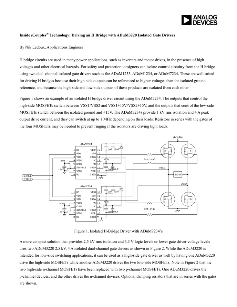
Inside iCoupler® Technology: Driving an H Bridge with ADuM3220 Isolated Gate Drivers By Nik Ledoux, Applications Engineer H bridge circuits are used in many power applications, such as inverters and motor drives, in the presence of high voltages and other electrical hazards. For safety and protection, designers can isolate control circuitry from the H bridge using two dual-channel isolated gate drivers such as the ADuM1233, ADuM1234, or ADuM7234. These are well suited for driving H bridges because their high-side outputs can be referenced to higher voltages than the isolated ground reference, and because the high-side and low-side outputs of these products are isolated from each other Figure 1 shows an example of an isolated H bridge driver circuit using the ADuM7234. The outputs that control the high-side MOSFETs switch between VSS1/VSS2 and VSS1+15V/VSS2+15V, and the outputs that control the low-side MOSFETs switch between the isolated ground and +15V. The ADuM7234s provide 1 kV rms isolation and 4 A peak output drive current, and they can switch at up to 1 MHz depending on their loads. Resistors in series with the gates of the four MOSFETs may be needed to prevent ringing if the isolators are driving light loads. Figure 1. Isolated H-Bridge Driver with ADuM7234’s A more compact solution that provides 2.5 kV rms isolation and 3.3 V logic levels or lower gate driver voltage levels uses two ADuM3220 2.5 kV, 4 A isolated dual-channel gate drivers as shown in Figure 2. While the ADuM3220 is intended for low-side switching applications, it can be used as a high-side gate driver as well by having one ADuM3220 drive the high-side MOSFETs while another ADuM3220 drives the two low-side MOSFETs. Note in Figure 2 that the two high-side n-channel MOSFETs have been replaced with two p-channel MOSFETs. One ADuM3220 drives the p-channel devices, and the other drives the n-channel devices. Optional damping resistors that are in series with the gates are shown. The high-side ADuM3220 switches the p-channel MOSFET’s gates from Vbridge to Vbridge – 5.1 V. The anode of a 5.1 V Zener diode is the ground reference for the high-side ADuM3220. This node is bypassed to the isolated ground with 0.1 µF and 10 µF capacitors. RBIAS provides bias current for the Zener. Its size depends on the maximum current that the high-side ADuM3220 will draw and the value of Vbridge. The maximum current depends on the application’s switching frequency and the size of the p-channel MOSFETs. The Zener diode should be chosen based on the desired gate drive voltage and the power dissipation that it will experience when the ADuM3220 draws low current levels from Vbridge, causing most of the current flowing into RBIAS to also flow through the diode. Here is an example of how to choose RBIAS with Vbridge = 24 V, 5 V gate drive levels (5.1V Zener), a 1 MHz switching frequency and 20 nC of gate charge at Vgs = 5V . First, the gate capacitance needs to be calculated. C = Q/V = 20 nC/5V = 4 nF where C = gate capacitance, Q = gate charge, V = final Vgs The current needed to drive these gates then needs to be calculated and added to the ADuM3220’s quiescent current. This represents the minimum bias current for the Zener diode: I = CVF = 4 nF(5 V)(1 MHz) = 20 mA where C = gate capacitance, V = Vgs, F = switching frequency The ADuM3220’s maximum VDD2 quiescent current is 10 mA. Therefore, the Zener diode needs to be biased to at least 30 mA. Since Vbridge is 24 V and a 5.1 V Zener is used, RBIAS should be no more than 630 Ω. RBIAS(max) = (Vbridge-VZener)/I = (24 V-5.1 V)/30 mA = 630 Ω Figure 2. Isolated H-Bridge Driver with ADuM3220’s In addition to the higher isolation rating (2.5 kV rms vs. 1 kV rms) and ability to use 3.3 V logic levels, the circuit in Figure 2 also has a wider output voltage range than the circuit in Figure 1: 4.5 V to 18 V instead of 12 V to 18 V. Perhaps more importantly, it also needs only about half of the board space as the Figure 1 circuit, since two 8-SOICs replace two narrow-body 16-SOICs. This does not even include the space that is saved by its less complicated power supply requirements. There are some caveats that the circuit designer should consider. The first is that it replaces the high-side switches with p-channel MOSFETs. For some applications this may be impractical because of their higher gate charge and rds(on) disadvantages relative to n-channel MOSFETs. Another caveat is related to the default LOW outputs of the ADuM3220. If the input side is unpowered, VOA and VOB will be driven low to GNDA and GNDB. This switches off the n-channel MOSFETs and switches on the p-channel MOSFETs. No cross-conduction will occur once the outputs settle because the low-side switches are off, but Vbridge will be applied to each terminal of the load. Figure 3 and Figure 4 show the results of a test circuit that we built to illustrate this application of the ADuM3220. The H bridge is set up to switch between ±16 V at 1 MHz. Figure 3 shows the outputs of the four gate drive signals. Figure 4 shows the control signals and the H bridge’s output. The test circuit used two separate PCBs and had many parasitic effects from our prototyping techniques that degraded the measurements’ signal integrity. Good layout practices with short, wide gate drive traces and careful timing of the control signals will result in cleaner waveforms. It is important to connect bypass capacitors between the high side GND2 and the low side GND2. Additional setup details are below: Supplies: Vbridge = 16 V, VDD1 = 3.3 V Components: 1N4733A Zener (5.1 V) FD4141 P-Channel MOSFETs FD8447L N-Channel MOSFETs RBIAS = 200 Ω 1 Ω series gate resistors Thus, two ADuM3220’s can be used instead of full-bridge drivers to switch an H bridge at frequencies up to 1 MHz. This gate drive scheme is a potential solution where 2.5 kV rms isolation with 3.3V logic levels, 4 A of peak drive current, or output voltages as low as 4.5 V are required. It also uses significantly less space than two half-bridge drivers, so it is appropriate for designs where board space is critical. CH1/2 = VOA/VOB of low-side ADuM3220 (Vgs of N-channel MOSFETs) CH 3/4 = VOA/VOB of high-side ADuM3220 Figure 3. ADuM3220 Outputs CH1/CH2 = CTRL1 (VIA) / CTRL2 (VIB) CH3 = VDS of NMOS driven by VOA Figure 4. H-Bridge Output ©2011 Analog Devices, Inc. All rights reserved. Trademarks and registered trademarks are the property of their respective owners. T09785-0-3/11

