INCREASE DYNAMIC RANGE OF SAR ADCS USING OVERSAMPLING TECHNICAL ARTICLE
advertisement
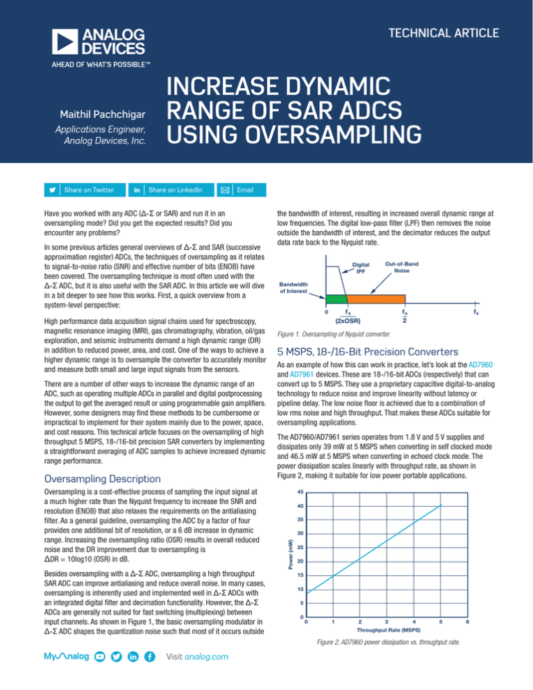
TECHNICAL ARTICLE Applications Engineer, Analog Devices, Inc. | Share on Twitter | Share on LinkedIn |Email Have you worked with any ADC (Δ-Σ or SAR) and run it in an oversampling mode? Did you get the expected results? Did you encounter any problems? In some previous articles general overviews of Δ-Σ and SAR (successive approximation register) ADCs, the techniques of oversampling as it relates to signal-to-noise ratio (SNR) and effective number of bits (ENOB) have been covered. The oversampling technique is most often used with the Δ-Σ ADC, but it is also useful with the SAR ADC. In this article we will dive in a bit deeper to see how this works. First, a quick overview from a system-level perspective: High performance data acquisition signal chains used for spectroscopy, magnetic resonance imaging (MRI), gas chromatography, vibration, oil/gas exploration, and seismic instruments demand a high dynamic range (DR) in addition to reduced power, area, and cost. One of the ways to achieve a higher dynamic range is to oversample the converter to accurately monitor and measure both small and large input signals from the sensors. There are a number of other ways to increase the dynamic range of an ADC, such as operating multiple ADCs in parallel and digital postprocessing the output to get the averaged result or using programmable gain amplifiers. However, some designers may find these methods to be cumbersome or impractical to implement for their system mainly due to the power, space, and cost reasons. This technical article focuses on the oversampling of high throughput 5 MSPS, 18-/16-bit precision SAR converters by implementing a straightforward averaging of ADC samples to achieve increased dynamic range performance. Oversampling Description Oversampling is a cost-effective process of sampling the input signal at a much higher rate than the Nyquist frequency to increase the SNR and resolution (ENOB) that also relaxes the requirements on the antialiasing filter. As a general guideline, oversampling the ADC by a factor of four provides one additional bit of resolution, or a 6 dB increase in dynamic range. Increasing the oversampling ratio (OSR) results in overall reduced noise and the DR improvement due to oversampling is ΔDR = 10log10 (OSR) in dB. Besides oversampling with a Δ-Σ ADC, oversampling a high throughput SAR ADC can improve antialiasing and reduce overall noise. In many cases, oversampling is inherently used and implemented well in Δ-Σ ADCs with an integrated digital filter and decimation functionality. However, the Δ-Σ ADCs are generally not suited for fast switching (multiplexing) between input channels. As shown in Figure 1, the basic oversampling modulator in Δ-Σ ADC shapes the quantization noise such that most of it occurs outside the bandwidth of interest, resulting in increased overall dynamic range at low frequencies. The digital low-pass filter (LPF) then removes the noise outside the bandwidth of interest, and the decimator reduces the output data rate back to the Nyquist rate. Digital IPF Out-of-Band Noise Bandwidth of Interest fs 2 fs (2xOSR) 0 fs Figure 1. Oversampling of Nyquist converter. 5 MSPS, 18-/16-Bit Precision Converters As an example of how this can work in practice, let’s look at the AD7960 and AD7961 devices. These are 18-/16-bit ADCs (respectively) that can convert up to 5 MSPS. They use a proprietary capacitive digital-to-analog technology to reduce noise and improve linearity without latency or pipeline delay. The low noise floor is achieved due to a combination of low rms noise and high throughput. That makes these ADCs suitable for oversampling applications. The AD7960/AD7961 series operates from 1.8 V and 5 V supplies and dissipates only 39 mW at 5 MSPS when converting in self clocked mode and 46.5 mW at 5 MSPS when converting in echoed clock mode. The power dissipation scales linearly with throughput rate, as shown in Figure 2, making it suitable for low power portable applications. 45 40 35 30 Power (mW) Maithil Pachchigar INCREASE DYNAMIC RANGE OF SAR ADCS USING OVERSAMPLING 25 20 15 10 5 0 0 1 2 3 4 5 Throughput Rate (MSPS) Figure 2. AD7960 power dissipation vs. throughput rate. Visit analog.com 6 2 Increase Dynamic Range of SAR ADCs Using Oversampling ADP7102 +12 V +5 V ADP7104 ADP2300 –VS = –2.5 V +7 V ADP124 +5 V +7 V ADR4550 +12 V Wall-Wart +5 V AD8031 +1.8 V 0 V to 5 V VCM +12 V REFIN REF VDD1 VDD2 VIO CNV± AD4899-1 AIN+ –VS IN+ USB Port PC 100 𝛀 D± 100 𝛀 DCO± 100 𝛀 SP-6 FPGA XC6SLX25 DSP BF522 AD7960/61 Signal Generator +7 V Audio Precision SYS-2702 Power Supply +VS IN− LVDS Interface AIN– AD4899-1 –VS 5 V to 0 V VCM VCM GND VCM CLK± 100 𝛀 +2.5 V +7 V SDP-H1 AD8031 Figure 3. Simplified schematic of AD7960/AD7961 evaluation setup (not all decoupling shown). AD7960/AD7961 Evaluation Setup Measurement Results The AD7960/AD7961 series converts the differential voltage of the antiphase analog inputs (IN+ and IN−) into a digital output. The analog inputs, IN+ and IN−, require a common-mode voltage equal to one half the reference voltage. The low noise and low power AD8031 amplifier buffers the 5 V reference voltage from the low noise and low drift ADR4550 and it also buffers the common-mode output voltage (VCM) of the AD7960/AD7961. The oversampling capability is implemented in the AD7960/AD7961 evaluation software using a simple averaging of the ADC output samples, meaning, and summing the number of ADC samples and dividing it by the oversampling ratio to get the increased dynamic range. This software allows the user to select the oversampling ratio up to 256 from the dropdown menu under the Configure tab as shown in Figure 4. The maximum dynamic range achieved is limited by the low frequency 1/f noise of the system, which starts to dominate at lower output data rates below 20 kSPS. The low noise and ultralow distortion ADA4899-1 is configured as a unity-gain buffer and drives the inputs of the AD7960/AD7961 with a 0 V to 5 V differential antiphase (180° out of phase with each other). The circuit uses supplies of +7 V and −2.5 V for the input ADA4899-1 drivers to minimize power dissipation and to achieve the optimum system distortion performance. The simplified schematic of evaluation setup using the EVAL-AD7960FMCZ daughter board and EVAL-SDP-H1 controller board is shown in Figure 3. In Part 1 of this article, we started looking at reducing noise, increasing dynamic range, and increasing the ENOB with a SAR ADC. The method is based on oversampling—commonly used on low speed, high resolution ∆-Σ ADCs—less commonly used elsewhere. We continue by looking at some test results with a SAR ADC using an evaluation board and its software. In Part 2, we will continue our look at the AD7960/AD796. We will also look at the available evaluation board and software that can provide analysis. We’ll see how well these ADCs do or do not perform. The evaluation board makes it easy to see performance by looking at the FFT output from the ADCs. Figure 4. AD7960/AD7961 evaluation software panel. Visit analog.com A spectrum of the signal and the flat noise from dc to fs/2 in Figure 5 and Figure 6 shows that the noise can be filtered to fs/(2 × OSR) to improve the dynamic range and SNR. In this case, the oversampled dynamic range is the ratio of the peak signal power to the noise power measured in the ADC output FFT from dc up to fs/(2 × OSR), where fs is the ADC sample rate. The AD7960 and AD7961 achieve a typical dynamic range of 100 dB and 96 dB, respectively, using a 5 V reference as specified in the data sheet, so in theory, we should see a 24 dB increment in the dynamic range due to oversampling by 256. In reality, the measured oversampled dynamic ranges of these parts are 122 dB and 119 dB, respectively, with no input signal when oversampled by 256× at output data rate of 19.53 kSPS, which shows a 1 dB to 2 dB degradation in the dynamic range from the theoretical calculation. This is limited by the low frequency noise coming from signal chain components, input source, and printed circuit board. With a 1 kHz full-scale sine wave input signal, these parts achieve oversampled SNR of roughly 111 dB and 110 dB, respectively. Figure 7 shows how the AD7960 achieves the increased dynamic range as the oversampling ratio is increased and output data rate is decreased. 125 19.5 Dynamic Range (dB) 120 115 110 105 5k 100 95 90 16 Figure 5. AD7960 oversampled FFT output with no input signal and fIN = 1 kHz (OSR = 256, REF = 5 V). 64 256 1024 Output Data Rate (kHz) 4096 Figure 7. AD7960 dynamic range vs. output data rate. Application Example MRI systems operate in the 1 MHz to 100 MHz RF frequency band, whereas computed tomography (CT) and digital X-ray operate in the 1016 Hz to 1018 Hz frequency range, subjecting patients to ionizing radiation that can damage living tissue. MRI gradient control systems demand a very high dynamic range, tight linearity, and fast response time from dc to tens of kilohertz, and their gradient must be precisely controlled within around 1 mA (1 ppm) in either analog or digital domain for enhanced image quality. Using an oversampled SAR ADC with good specifications (such as the AD7960) would allow design engineers to achieve the high dynamic range and meet the key requirements for MRI systems. Such systems need measurement repeatability and stability over long periods of time in a hospital or doctor’s office environment. The additional requirements that the design engineer should look for are high resolution, accuracy, low noise, fast refresh rates, and very low output drift. For more information on any of the above mentioned products visit www.analog.com/DAC. Figure 6. AD7961 oversampled FFT output with no input signal and with fIN = 1 kHz (OSR = 256, REF = 5 V). 3 About The Author Maithil Pachchigar is an applications engineer within the precision converters business unit at Analog Devices. He joined ADI in 2010 and supports the precision ADC product portfolio and customers in the industrial, instrumentation, medical, and energy segments. Having worked in the semiconductor industry since 2005, Maithil has published several technical articles. He received an M.S.E.E. degree from San Jose State University in 2006 and an M.B.A. from Silicon Valley University in 2010. He can be reached at maithil.pachchigar@analog.com. Online Support Community Engage with the Analog Devices technology experts in our online support community. Ask your tough design questions, browse FAQs, or join a conversation. ez.analog.com Analog Devices, Inc. Worldwide Headquarters Analog Devices, Inc. Europe Headquarters Analog Devices, Inc. Japan Headquarters Analog Devices, Inc. Asia Pacific Headquarters Analog Devices, Inc. One Technology Way P.O. Box 9106 Norwood, MA 02062-9106 U.S.A. Tel: 781.329.4700 (800.262.5643, U.S.A. only) Fax: 781.461.3113 Analog Devices, Inc. Wilhelm-Wagenfeld-Str. 6 80807 Munich Germany Tel: 49.89.76903.0 Fax: 49.89.76903.157 Analog Devices, KK New Pier Takeshiba South Tower Building 1-16-1 Kaigan, Minato-ku, Tokyo, 105-6891 Japan Tel: 813.5402.8200 Fax: 813.5402.1064 Analog Devices 5F, Sandhill Plaza 2290 Zuchongzhi Road Zhangjiang Hi-Tech Park Pudong New District Shanghai, China 201203 Tel: 86.21.2320.8000 Fax: 86.21.2320.8222 ©2015 Analog Devices, Inc. All rights reserved. Trademarks and registered trademarks are the property of their respective owners. Ahead of What’s Possible is a trademark of Analog Devices. TA12916-0-6/15 analog.com
