Electric Field Distribution in a Grating of a Folded Arrayed-Waveguide Multiplexer
advertisement
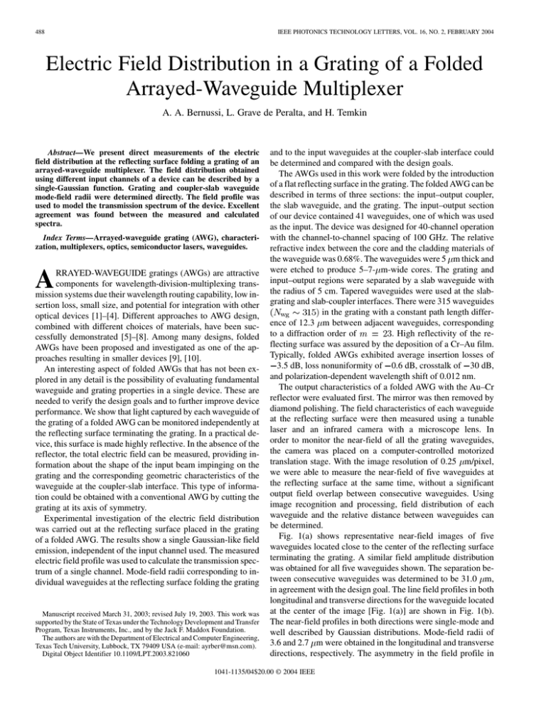
488 IEEE PHOTONICS TECHNOLOGY LETTERS, VOL. 16, NO. 2, FEBRUARY 2004 Electric Field Distribution in a Grating of a Folded Arrayed-Waveguide Multiplexer A. A. Bernussi, L. Grave de Peralta, and H. Temkin Abstract—We present direct measurements of the electric field distribution at the reflecting surface folding a grating of an arrayed-waveguide multiplexer. The field distribution obtained using different input channels of a device can be described by a single-Gaussian function. Grating and coupler-slab waveguide mode-field radii were determined directly. The field profile was used to model the transmission spectrum of the device. Excellent agreement was found between the measured and calculated spectra. Index Terms—Arrayed-waveguide grating (AWG), characterization, multiplexers, optics, semiconductor lasers, waveguides. A RRAYED-WAVEGUIDE gratings (AWGs) are attractive components for wavelength-division-multiplexing transmission systems due their wavelength routing capability, low insertion loss, small size, and potential for integration with other optical devices [1]–[4]. Different approaches to AWG design, combined with different choices of materials, have been successfully demonstrated [5]–[8]. Among many designs, folded AWGs have been proposed and investigated as one of the approaches resulting in smaller devices [9], [10]. An interesting aspect of folded AWGs that has not been explored in any detail is the possibility of evaluating fundamental waveguide and grating properties in a single device. These are needed to verify the design goals and to further improve device performance. We show that light captured by each waveguide of the grating of a folded AWG can be monitored independently at the reflecting surface terminating the grating. In a practical device, this surface is made highly reflective. In the absence of the reflector, the total electric field can be measured, providing information about the shape of the input beam impinging on the grating and the corresponding geometric characteristics of the waveguide at the coupler-slab interface. This type of information could be obtained with a conventional AWG by cutting the grating at its axis of symmetry. Experimental investigation of the electric field distribution was carried out at the reflecting surface placed in the grating of a folded AWG. The results show a single Gaussian-like field emission, independent of the input channel used. The measured electric field profile was used to calculate the transmission spectrum of a single channel. Mode-field radii corresponding to individual waveguides at the reflecting surface folding the grating Manuscript received March 31, 2003; revised July 19, 2003. This work was supported by the State of Texas under the Technology Development and Transfer Program, Texas Instruments, Inc., and by the Jack F. Maddox Foundation. The authors are with the Department of Electrical and Computer Engineering, Texas Tech University, Lubbock, TX 79409 USA (e-mail: ayrber@msn.com). Digital Object Identifier 10.1109/LPT.2003.821060 and to the input waveguides at the coupler-slab interface could be determined and compared with the design goals. The AWGs used in this work were folded by the introduction of a flat reflecting surface in the grating. The folded AWG can be described in terms of three sections: the input–output coupler, the slab waveguide, and the grating. The input–output section of our device contained 41 waveguides, one of which was used as the input. The device was designed for 40-channel operation with the channel-to-channel spacing of 100 GHz. The relative refractive index between the core and the cladding materials of the waveguide was 0.68%. The waveguides were 5 m thick and were etched to produce 5–7- m-wide cores. The grating and input–output regions were separated by a slab waveguide with the radius of 5 cm. Tapered waveguides were used at the slabgrating and slab-coupler interfaces. There were 315 waveguides in the grating with a constant path length difference of 12.3 m between adjacent waveguides, corresponding . High reflectivity of the reto a diffraction order of flecting surface was assured by the deposition of a Cr–Au film. Typically, folded AWGs exhibited average insertion losses of 3.5 dB, loss nonuniformity of 0.6 dB, crosstalk of 30 dB, and polarization-dependent wavelength shift of 0.012 nm. The output characteristics of a folded AWG with the Au–Cr reflector were evaluated first. The mirror was then removed by diamond polishing. The field characteristics of each waveguide at the reflecting surface were then measured using a tunable laser and an infrared camera with a microscope lens. In order to monitor the near-field of all the grating waveguides, the camera was placed on a computer-controlled motorized translation stage. With the image resolution of 0.25 m/pixel, we were able to measure the near-field of five waveguides at the reflecting surface at the same time, without a significant output field overlap between consecutive waveguides. Using image recognition and processing, field distribution of each waveguide and the relative distance between waveguides can be determined. Fig. 1(a) shows representative near-field images of five waveguides located close to the center of the reflecting surface terminating the grating. A similar field amplitude distribution was obtained for all five waveguides shown. The separation between consecutive waveguides was determined to be 31.0 m, in agreement with the design goal. The line field profiles in both longitudinal and transverse directions for the waveguide located at the center of the image [Fig. 1(a)] are shown in Fig. 1(b). The near-field profiles in both directions were single-mode and well described by Gaussian distributions. Mode-field radii of 3.6 and 2.7 m were obtained in the longitudinal and transverse directions, respectively. The asymmetry in the field profile in 1041-1135/04$20.00 © 2004 IEEE BERNUSSI et al.: ELECTRIC FIELD DISTRIBUTION IN A GRATING OF A FOLDED ARRAYED-WAVEGUIDE MULTIPLEXER (a) Amplitude (arb. units) (b) longit. transv. -15 -10 -5 0 5 distance (µm) 10 15 Fig. 1. (a) Near-field image of five waveguides at the grating reflecting surface of a 100-GHz folded AWG device, and (b) longitudinal and transverse line profiles for the waveguide at the center of image (a). 10 489 important to the performance of a folded device in which the input and output waveguides overlap. It should be remembered that the number of waveguides in the grating is finite and their separation is not zero. Not all of the light reaching the reflecting surface is thus collected, only the light captured by the grating. In order to estimate the loss resulting from the finite number of waveguides, known as the power truncation, we compared the integral of the total output field distribution (shown in Fig. 2) with the one of a Gaussian with the same width and peak amplitude but extended to infinity. An additional loss contribution of about 0.06 dB was estimated by truncating the number of grating waveguides to . This confirms that the number of waveguides used in the grating of our folded device is sufficient to assure low-loss AWG. The data of Fig. 2 enabled us to determine the mode-field radius corresponding to the near-field of the input waveguide at the interface between the input coupler and the slab waveguide and to calculate the output spectra of any channel. The passband spectrum of an AWG, for an output channel designed to collect the light with the wavelength , can be described as [11] 2 Amplitude (arb. units) (1) 101 100 input channel: marginal center 0 2 4 6 distance (mm) 8 Fig. 2. Field amplitude distribution at the grating–reflecting surface. The data is plotted using the center channel input waveguide () or a marginal channel input (). the two directions results from the rectangular cross section of waveguides in the grating. The measured mode-field radii obtained from Fig. 1 agrees quantitatively with those obtained m from beam-propagation simulation of a rectangular waveguide with the index step of 0.68%. Field distribution profiles at the reflecting surface obtained using the center channel and marginal channel inputs are shown in Fig. 2. The field distributions were obtained from the maximum of each individual waveguide near-field profile. A 1550-nm wavelength input was used in this experiment. The field profiles at the reflecting surface were essentially identical for the center and marginal channel inputs. For both cases, the field profile could be described by a single Gaussian function. The results of Fig. 2 show that the input light is efficiently captured by the tapered waveguides at the grating–slab interface even when the illumination, relative to the grating arc, is not symmetric, as is the case for marginal input channels. This is where is the spectral range in the vicinity of the channel’s center peak, is the effective refractive index of the grating waveguide, is the path length of the th grating waveguide, is the normalized field amplitude at the center of the and waveguide. The latter was obtained experimentally in Fig. 2. The spatial distribution (far-field) of light at the grating input corresponds to the spatial Fourier transform of the light intensity produced by a single waveguide at the coupler–slab interface (near-field) [12]. In the single Gaussian approximation, the and the far-field mode-field radii of the near-field are related through the expression [12] (2) where and are the radius and the refractive index of the AWG slab region, respectively. The far-field mode-field radius was obtained directly from the experimental data shown in Fig. 2 and a value of mm was determined. Substituting this value of into m for the waveguide beam at the (2), we obtain corresponds to the coupler–slab interface. This value of mode-field radius of the tapered waveguide at the slab–coupler interface. The tapers were designed to have cosine shape and the obtained here is in good agreement with beam propagation simulation. obtained from Using the design and the experimental Fig. 2, the optical power spectrum can be calculated from (1) for an ideal situation where random phase errors are absent. Without phase errors the calculated spectrum (not shown) coincides with the data at the principal maximum but the side lobes are well below the experimental background level. It is well known that phase errors affect primarily the side lobes of the 490 IEEE PHOTONICS TECHNOLOGY LETTERS, VOL. 16, NO. 2, FEBRUARY 2004 0 in good agreement with the design parameters. Our results show that the number of grating waveguides used and the taper geometry result in folded AWGs with low losses. The output spectrum of a single channel calculated using the measured grating field distribution profile was found to be in good agreement with the measurement. Exp. Intensity (dB) -10 Calc. -20 -30 REFERENCES -40 1548 [1] M. K. Smit, “New focusing and dispersive planar component based on an optical phased array,” Electron. Lett., vol. 24, pp. 385–386, 1988. [2] C. Dragone, “An N N optical multiplexer using a planar arrangement of two star couplers,” IEEE Photon. Technol. Lett., vol. 3, pp. 812–815, Sept. 1991. [3] A. Himeno, K. Kato, and T. Miya, “Silica-based planar lightwave circuits,” IEEE J. Select. Topics Quantum Electron., vol. 4, pp. 913–924, Nov./Dec. 1998. [4] M. K. Smit and C. van Dam, “PHASAR-based WDM-devices: Principles, design and applications,” IEEE J. Select. Topics Quantum Electron., vol. 2, pp. 236–250, June 1996. [5] C. Dragone, “Efficient techniques for widening the passband of a wavelength router,” IEEE J. Lightwave Technol., vol. 16, pp. 1895–1906, Oct. 1998. [6] M. Zirngibl, C. H. Joyner, and P. C. Chou, “Polarization compensated waveguide grating router on InP,” Electron. Lett., vol. 31, pp. 1662–1664, 1995. [7] C. K. Nadler, E. K. Wildermuth, M. Lanker, W. Hunziker, and H. Melchior, “Polarization insensitive, low-loss, low-crosstalk wavelength multiplexer modules,” IEEE J. Select. Topics Quantum Electron., vol. 5, pp. 1407–1412, Sept./Oct. 1999. [8] M. B. J. Diemeer, L. H. Spickman, R. Ramsamoedj, and M. K. Smit, “Polymeric phase array wavelength multiplexer operating around 1550 nm,” Electron. Lett., vol. 32, pp. 1132–1133, 1996. [9] C. Dragone, “Efficient Reflective Multiplexer Arrangement,” U.S. Patent 5 450 511, Sept. 12, 1995. [10] J. B. D. Soole, M. R. Amersfoort, H. P. LeBlanc, A. Rajhel, C. Caneau, C. Youtsey, and I. Adesida, “Compact polarization independent InP reflective arrayed waveguide grating filter,” Electron. Lett., vol. 32, pp. 1769–1771, 1996. [11] C. D. Lee, W. Chen, Q. Wang, Y. J. Chen, W. T. Beard, D. Stone, R. F. Smith, R. Mincher, and I. R. Stewar, “The role of photomask resolution on the performance of arrayed-waveguide grating devices,” J. Lightwave Technol., vol. 19, pp. 1726–1733, Nov. 2001. [12] P. Muñoz, D. Pastor, and J. Capmany, “Modeling and design of arrayed waveguide gratings,” J. Lightwave Technol., vol. 20, pp. 661–674, Apr. 2002. [13] K. Okamoto, Fundamentals of Optical Waveguides. New York: Academic, 2000, ch. 9, pp. 341–400. 2 1550 1552 Wavelength (nm) Fig. 3. Calculated (—) and measured ( ) spectrum of a single output channel. transmission spectra [13]. These errors are present in the grating as a result of the fabrication process uncertainties. The effects of phase errors have been modeled assuming random variation and substituting in in the path length (1) [11]. Fig. 3 shows a comparison of measured and calculated transmission spectra of a single channel of a folded AWG. A good agreement between the calculated and measured spectra is obtained using the Gaussian field profile shown in Fig. 2 and (1) in the range of a uniform pseudorandom distribution of m. This corresponds to a path-length distribution with a standard deviation of 30 nm and a maximum fluctuation of 0.1 m. The random path-length errors used in the simulation represent the phase errors introduced during the AWG fabrication process. In summary, the electric field distribution at the reflecting surface of a folded AWG was investigated. Mode-field radii of the grating waveguides were measured directly. The overall field distribution exhibited a single Gaussian profile. Our results showed similar field profiles when either marginal or central waveguides were used as inputs. From the analysis of the field profile, we derive mode-field radii corresponding to the beam at the coupler–slab interface. All of the field radii were found to be
