Process development of silicon-silicon carbide hybrid structures for micro-engines (January 2002) D. Choi
advertisement
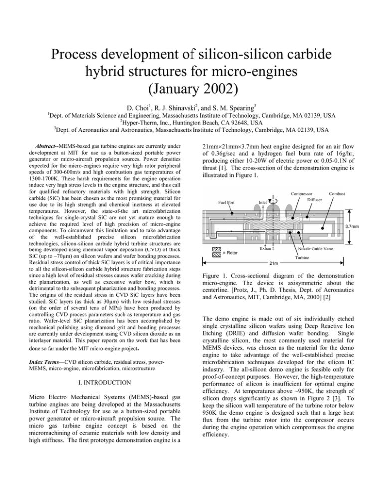
Process development of silicon-silicon carbide hybrid structures for micro-engines (January 2002) D. Choi1, R. J. Shinavski2, and S. M. Spearing3 1 Dept. of Materials Science and Engineering, Massachusetts Institute of Technology, Cambridge, MA 02139, USA 2 Hyper-Therm, Inc., Huntington Beach, CA 92648, USA 3 Dept. of Aeronautics and Astronautics, Massachusetts Institute of Technology, Cambridge, MA 02139, USA Abstract--MEMS-based gas turbine engines are currently under development at MIT for use as a button-sized portable power generator or micro-aircraft propulsion sources. Power densities expected for the micro-engines require very high rotor peripheral speeds of 300-600m/s and high combustion gas temperatures of 1300-1700K. These harsh requirements for the engine operation induce very high stress levels in the engine structure, and thus call for qualified refractory materials with high strength. Silicon carbide (SiC) has been chosen as the most promising material for use due to its high strength and chemical inertness at elevated temperatures. However, the state-of-the art microfabrication techniques for single-crystal SiC are not yet mature enough to achieve the required level of high precision of micro-engine components. To circumvent this limitation and to take advantage of the well-established precise silicon microfabrication technologies, silicon-silicon carbide hybrid turbine structures are being developed using chemical vapor deposition (CVD) of thick SiC (up to ~70µm) on silicon wafers and wafer bonding processes. Residual stress control of thick SiC layers is of critical importance to all the silicon-silicon carbide hybrid structure fabrication steps since a high level of residual stresses causes wafer cracking during the planarization, as well as excessive wafer bow, which is detrimental to the subsequent planarization and bonding processes. The origins of the residual stress in CVD SiC layers have been studied. SiC layers (as thick as 30µm) with low residual stresses (on the order of several tens of MPa) have been produced by controlling CVD process parameters such as temperature and gas ratio. Wafer-level SiC planarization has been accomplished by mechanical polishing using diamond grit and bonding processes are currently under development using CVD silicon dioxide as an interlayer material. This paper reports on the work that has been done so far under the MIT micro-engine project. Index Terms—CVD silicon carbide, residual stress, powerMEMS, micro-engine, microfabrication, microstructure I. INTRODUCTION Micro Electro Mechanical Systems (MEMS)-based gas turbine engines are being developed at the Massachusetts Institute of Technology for use as a button-sized portable power generator or micro-aircraft propulsion source. The micro gas turbine engine concept is based on the micromachining of ceramic materials with low density and high stiffness. The first prototype demonstration engine is a 21mm×21mm×3.7mm heat engine designed for an air flow of 0.36g/sec and a hydrogen fuel burn rate of 16g/hr, producing either 10-20W of electric power or 0.05-0.1N of thrust [1]. The cross-section of the demonstration engine is illustrated in Figure 1. Fuel Port Compressor Diffuser Inlet Combust 3.7mm Exhau Nozzle Guide Vane = Rotor Turbine 21m Figure 1. Cross-sectional diagram of the demonstration micro-engine. The device is axisymmetric about the centerline. [Protz, J., Ph. D. Thesis, Dept. of Aeronautics and Astronautics, MIT, Cambridge, MA, 2000] [2] The demo engine is made out of six individually etched single crystalline silicon wafers using Deep Reactive Ion Etching (DRIE) and diffusion wafer bonding. Single crystalline silicon, the most commonly used material for MEMS devices, was chosen as the material for the demo engine to take advantage of the well-established precise microfabrication techniques developed for the silicon IC industry. The all-silicon demo engine is feasible only for proof-of-concept purposes. However, the high-temperature performance of silicon is insufficient for optimal engine efficiency. At temperatures above ~950K, the strength of silicon drops significantly as shown in Figure 2 [3]. To keep the silicon wall temperature of the turbine rotor below 950K the demo engine is designed such that a large heat flux from the turbine rotor into the compressor occurs during the engine operation which compromises the engine efficiency. purpose of increasing its stiffness and resistance to creep and oxidation. The negative mold concept consists of fabricating the inverse pattern of the turbine rotor into the silicon substrate and then filling the mold cavity with thick CVD SiC followed by the dissolution of the silicon mold using HF/HNO3 to yield a free standing SiC turbine rotor. Strength (MPa) 10000 1000 Silicon CVD Silicon Carbide (a) 100 10 600 (b) Hub 800 1000 1200 1400 1600 Blades 1800 Temperature (K) Figure 2. Strength as a function of temperature for Si and CVD SiC. Trends based on literature data from Pearson 1957, Mura 1996, Castaing 1981, Patel 1963, Huff 1993, Pickering 1990, Hirai & Sasaki 1991, Chen 1999. [Lohner, K., S.M. Thesis, Dept. of Aeronautics and Astronautics, MIT, Cambridge, MA, 1999] [3] The low strength of silicon at elevated temperatures and the necessity of achieving the desired overall high engine efficiency dictate the critical need for developing better refractory materials. Power densities expected for the microengine require combustor exit temperatures of 13001700K and rotor peripheral speeds of 300-600m/s. These operating conditions induce high stress levels in the engine structure, and thus require qualified refractory materials with high strength. Therefore, one of the essential material selection criteria for the microengine is σf(T)/ρ, where σf(T) is the tensile fracture or yield strength as a function of temperature and ρ is the density [4]. In addition to the above strength criterion, creep and oxidation resistance at high temperatures should be taken into account as well. Based on these criteria for material selection, refractory ceramics, such as silicon carbide (SiC) and silicon nitride (SiNx), had been suggested for alternate materials for the turbine structure. SiC has been identified as the most promising candidate for use in the near future due to its high stiffness, toughness, and strength at elevated temperatures. However, techniques for microfabricating single crystalline SiC to the level of high precision needed for the microengine are not currently available due primarily to the lack of precise and fast SiC etching techniques. To circumvent this limitation, Chemical Vapor Deposition (CVD) of SiC coatings over etched silicon molds using the ‘Strawman’ process concepts had been suggested to fabricate the SiC turbine structure and their feasibility has been studied [3]. The processing concepts were evaluated in terms of conformality, process integration, the level of residual stress, and the absence of structural defects such as micro-cracks. Three process concepts, positive mold, negative mold, and hybrid mold configurations, were studied as shown in Figure 3. The positive mold concept is to deposit a thin (<10µm) layer of CVD SiC over a fabricated silicon turbine rotor for the (c) Key: = SiC = Si Figure 3. Positive, negative, and Si/SiC hybrid turbine rotor configurations. (a) Positive, (b) Negative, and (C) Si/SiC hybrid structure. [Lohner, K., MRS Proceedings, Vol. 546, 1998] [10] The hybrid mold concept is to combine the CVD SiC deposition with post-deposition processes to yield the turbine rotor that contains SiC reinforcements in strategic locations to increase its strength and stiffness. Considering the microfabrication difficulties in making an all-SiC turbine rotor and the process compatibility with other microengine fabrication processes such as wafer bonding and turbine release, it has been concluded that the Si/SiC hybrid concept is the most promising approach to improving microengine performance by increasing the maximum operating temperature using already proven fabrication technologies. The initial Finite Element (FE) study has shown that the Si/SiC hybrid structures can significantly increase the operating power levels of the microengine by increasing the allowable working temperature by 150-200K [5]. Three-dimensional FE simulations for the Si/SiC hybrid turbine rotor have also been performed with a refined model combining the turbine disc and blades in order to verify the previous structural analysis where the hybrid turbine and disc were considered as separate bodies. Four different geometrical configurations were considered in the 3-D simulation and the 3-D FE simulation results confirm the potential of the Si/SiC hybrid structure concept for improving engine efficiency by increasing the maximum allowable working temperature. The Si/SiC hybrid spool having a disc with 30% SiC reinforcement and hollow blades designed to have reduced turbine-to-compressor contact areas was shown to enhance the microengine efficiency through a 1-D cycle analysis performed by the system engineers [6]. An outline of the necessary processing steps required to create a Si/SiC hybrid turbine rotor is shown in Figure 4. Etch disc Planarization / Polishing SiC hybrid turbine rotor and compressor CVD SiC SiC/Si Bonding Figure 4. Key fabrication steps for the Si/SiC hybrid turbine rotor structure. In this paper, the efforts that have been made to achieve the Si/SiC hybrid turbine structures will be discussed with emphasis on process developments in the context of the overall micro-engine development program. II. BACKGROUND Residual stress control by changing CVD process variables is of critical importance to all the Si/SiC hybrid structure fabrication steps since a high level of residual stresses has been shown to cause wafer cracking during the planarization, as well as excessive wafer bow, which is detrimental to the subsequent planarization and bonding processes. Therefore, the first requirement is to understand the origins of the residual stresses in CVD SiC on the basis of the correlation between SiC microstructures and CVD process conditions. A. Origins of residual stresses in deposited materials such as CVD SiC Low Pressure Chemical Vapor Deposition (LPCVD) of polycrystalline SiC benefits from the ability to grow β-SiC on large-area Si substrates and the simplicity of the deposition procedure. However, the residual stress associated with the deposition and cooling processes may limit its applicability to the fabrication of MEMS devices. That is, a higher level of residual stress makes it very challenging to deposit thick SiC layers required for reinforcement of the Si/SiC hybrid turbine structure. Also, excessive residual stress causes a significant wafer bow that is not tolerable during the subsequent wafer planarization and bonding processes. Therefore, it is critical to understand the basic mechanisms of residual stress generation during the deposition process to be able to control the residual stress to a level that would not present a problem for subsequent fabrication processes. The stress development in polycrystalline films is associated with both thermal and intrinsic stresses. Thermal stress develops in the SiC film during cooling to room temperature due to the thermal mismatch between the SiC and the Si substrate. Intrinsic stress, the second contribution to the total residual stress, is more interesting since it reflects the growth of the film in a way that is not very well understood even at present [7]. Intrinsic stresses develop during the deposition process and are produced by the existence of grain boundaries or defects such as dislocations, voids, etc [8]. Grain boundaries and impurities such as oxygen and water vapors are the most well-known sources of intrinsic tensile and compressive stresses, respectively. The presence of grain boundaries in polycrystalline materials introduces tensile stresses due to attractive atomic forces acting across the grain boundaries [7, 9]. Compressive intrinsic stress is generally observed in metal films prepared under the conditions that favor energetic particles striking the growing film. When the growing film is bombarded by energetic atoms, the defects will include the gas atoms in either interstitial positions or more likely in lattice positions. Theses positions are coupled with self-interstitial defects formed when the gas atoms in the interstitial positions push neighboring lattice-sited atoms into interstitial positions and occupy the vacancies they create [11]. Thus the contribution of the gas atoms that do not escape from the film during the deposition will be to generate a compressive stress. This atomic peening is generally operative in low-pressure magnetron sputtering or ion beam sputtering. However, for the cases of nonenergetic particle depositions, impurities such as oxygen, water vapor, and hydrogen gases, have been observed to be the principal sources for intrinsic compression. For example, it has been shown that water vapor and oxygen produce compressive stress in silicon monoxide and aluminum, respectively [12]. B. Basic microfabrication steps for the Si/SiC hybrid turbine structure 1) LPCVD SiC CVD SiC is deposited on 4″ (100) silicon wafers by the thermal decomposition of vaporized methyltrichlorosilane (MTS) using hydrogen as a carrier gas at elevated temperature and sub-atmospheric pressures by HyperTherm, Inc., sub-contractor for the microengine project, according to the following chemical reaction [3, 13]. CH3SiCl3 + αH2 → SiC + 3HCl + αH2 where α is the molar ratio of H2 to CH3SiCl3. The deposition temperature ranges from 950°C to 1300°C and typically crystalline β-SiC with a zinc-blende structure is produced in this temperature range. The deposition rate is between 2 and 10µm per hour. Material characterization has shown that the CVD SiC produced by Hyper-Therm meets most of the property requirements for the microengine such as high strength, conformality, and low surface roughness. However, the high level of residual stress in CVD SiC makes wafer-level fabrication very challenging since the residual stress in SiC causes wafer bow and this induced wafer curvature makes it very difficult to planarize the wafers without cracking. 2) SiC planarization After deposition of SiC, the unnecessary parts of the SiC coatings should be removed by a polishing process for the subsequent wafer bonding process. For good wafer bonding, it is required to achieve very high degree of surface smoothness after planarization. For the case of SiSi wafer bonding process, it has been experimentally observed that the wafers should have a roughness of no greater than about 10Å [19]. SiC presents many challenges for wafer surface finishing because of its very high hardness and remarkable chemical inertness. Existing surface polishing techniques can be categorized as purely mechanical, chemomechanical, or etching. Mechanical polishing of SiC wafers primarily uses diamond polishing compounds mixed with water. Chemical-Mechanical Polishing (CMP) combines mechanical polishing with chemical etching actions, and has been shown to be very effective and can achieve very high smoothness [15]. However, due to the chemical inertness of SiC, CMP is not yet available to improve the surface smoothness of SiC to the level adequate for direct wafer bonding. Thus, the current planarization technique adopted in this research uses only mechanical polishing using diamond grit. However, diamond grit unavoidably results in a very rough, hill-and-valley-like surface structure since it achieves material removal through plastic deformation and fracture events. The current SiC planarization technique suffers from very low yield due to the wafer bow caused by residual stresses in SiC. 3) Wafer bonding process After planarization, the polished SiC wafer is bonded to a silicon wafer that will be fabricated into a compressor by DRIE. For successful wafer bonding, the wafer surfaces to be bonded should be sufficiently clean, smooth, and flat. Unfortunately, these conditions cannot be satisfied by the planarized SiC wafers. Therefore, for direct wafer bonding, an interlayer material such as CVD oxide or polycrystalline silicon should be first deposited on the rough surface of the polished SiC wafers to fill the grooves and then polished to a surface smoothness of better than ~5Å [16]. All the wafers to be bonded should be cleaned immediately before wafer contact using H2O2-based standard RCA wet cleaning process to remove any organic and metallic contaminants on the wafer surfaces. The RCA cleaning process also makes the wafer surface to become hydrophilic, which is required for spontaneous bonding upon wafer contact. III. RESIDUAL STRESS CALCULATION In the case of thin film materials deposited on substrates, the well-known Stoney formula can be utilized to calculate the residual stresses in the films. The SiC coatings for the micro-engine applications, however, are very thick and thus the Stoney formula cannot be used. Moreover, the necessity to control their residual stress states calls for a better method by which each component of the residual stresses can be separated from one another. In general, the residual stress development in the polycrystalline films deposited on substrates at high temperatures is associated with both thermal and intrinsic stresses. Due to the high deposition temperature and the difference in thermal expansion coefficients between the film and substrate thermal stress develops in the films during cool down to room temperature after deposition. Intrinsic stresses are defined as the stresses that develop during the deposition processes and are observed to be induced by the existence of defects such as dislocations, voids, grain boundaries, and etc. or impurities in the films [18, 19]. To separate the intrinsic stress component in the SiC inherent to the CVD process from the thermally induced stresses laminated composite plate methods have been utilized. In classical lamination theory, a laminate is two or more laminae bonded together to act as an integral structural element and the general constitutive equation relating the elastic properties of a material with the forces and moments is give by: N A B ε M = B D κ (1) where [A], [B], and [D] are in-plane stiffness matrices for a laminate, coupling stiffness matrix for a laminate, and bending stiffness matrix for a laminate respectively, and ε and κ are strain and curvature of the laminate. N and M are stress and moment resultants acting on a laminate that are obtained by integration of the stress and moment components in each layer through the laminate thickness [21]. To calculate both the thermal and intrinsic stresses, this general equation of matrices should be solved two times, firstly for the thermal stress and secondly for the intrinsic stress. The thermal stress of the SiC can be calculated after the thermal component of in-plain strain and thermal curvature are obtained by solving this equation. This equation should be solved once again for the intrinsic stress component by assuming that all the strains in the SiC, except the thermal induced strain are due to intrinsic forces generated during the deposition process. The intrinsic inplane strain is therefore given by the difference between the total in-plane strain and the thermal in-plane strain. The intrinsic curvature can also be obtained from the difference between the total curvature that is known from the laser profilometry and the thermally induced curvature likewise. Thus the intrinsic stress state in the SiC is given by: −1 ε total − ε thermal A B N intrinsic = κ total − κ thermal B D M intrinsic (2) where the total in-plane strain (εtotal ) and the intrinsic stress resultant (Nintrinsic) are unknown quantities. By describing Mintrinsic properly as a function of Nintrinsic the two unknowns can be calculated and used to calculate the intrinsic residual stress in the SiC layers. The total residual stress can be obtained simply by the summation of the calculated thermal and intrinsic stresses. IV. RESIDUAL STRESS CONTROL OF CVD SiC Various CVD conditions were examined to study relationships between residual stresses and CVD process conditions with the aim to achieve lower levels of residual stress. One of the efforts was to examine the deposition conditions as a function of the molar gas ratio α (H2:MTS). Figure 1 shows the variations of the thermal stress and the intrinsic stress as well as the total stress with the gas ratio α. 400 300 Residual Stress in SiC (MPa) 200 100 0 -100 -200 -300 impurity levels of the SiC coatings. However, the results showed that they contained no detectable amounts of impurities other than oxygen and even the oxygen contents were very low. Moreover, no trend or strong correlation between the residual compressive stress state and oxygen content was observed. It is thought that the residual stress is associated with the low atomic mobility of incoming SiC atoms during the CVD process, but definitely more work should be done to understand the sources of the compressive stresses in SiC. In parallel with homogeneous SiC coatings, a SiC/SiN layered material is being developed in collaboration with Hyper-Therm with the aim of producing a locally stress-balanced material. In addition to the stress magnitude, residual stress gradient also matters during the polishing process. Even if one could achieve a single ‘SiC target thickness’ with zero net residual stress, during the planarization, the wafer curvature or bow could still change as the SiC is removed from the wafer because of the stress gradient. A SiC/SiNx layered material could be a solution to the problem since SiNx has been shown to be always in residual tension. Therefore, SiC/SiNx films composed of alternating compressive SiC and tensile SiNx layers could display near-zero stress and stress gradient, depending on the relative thickness of each layer under given process conditions. -400 -500 -600 1 2 3 4 5 6 7 8 9 10 SiNx Gas Ratio Thermal Stress Intrinsic Stress SiC Net Stress Figure 5. Residual stress variance with gas ratio α (H2:MTS) The thermal stresses are nearly constant since all the data points were obtained from the SiC layers deposited at the same temperature. The small variations found in the thermal stresses are due to small variations in thicknesses of SiC coatings and silicon substrates. The plot shows that it is possible to control the intrinsic stresses and ultimately obtain a near net-zero total residual stress state by changing the gas ratio α. The low level of residual stress should also be able to be achieved by controlling other CVD process parameters such as deposition temperature and gas pressures, either by changing each of the process parameters or by varying two or more process variables at a time. The intrinsic residual stresses in SiC are compressive while the thermal stresses are tensile as shown in Figure 5. The tensile nature of the thermal stresses can be understood by the fact that the average thermal expansion coefficient of SiC is greater than that of Si in the temperature ranges of interest. However, the origins of the compressive (intrinsic) stresses are not yet understood. In several thin film materials, incorporation of impurities such as oxygen or hydrogen in grain boundaries has been reported to cause residual compression [20]. Secondary Ion Mass Spectrometry (SIMS) has been performed to investigate the 2 µm Figure 6. TEM image of SiC/SiNx layered material If the residual stresses between a SiC layer and an interrupting SiNx layer, balance to net-zero over a very small thickness, the wafer curvature should not change during the planarization. A TEM picture of an SiC/SiNx coating is shown in Figure 6. The interrupting thin layer of silicon nitride (denoted SiNx because crystallinity and stoichiometry is not confirmed) can be formed by the addition of ammonia to process gas streams. The cyclic gas switching is accomplished through an automated valve system and the switching time is about 500 milliseconds. It has been observed that only SiNx is deposited when the ammonia to MTS ratio exceeds two [13]. The wafers coated with SiC/SiNx were very flat compared with the wafers coated with SiC only, but no systematic study on the residual stress of each SiNx or SiC layer has yet been performed. V. PLANARIZATION AND SiC WAFER BONDING SiC wafer-level planarization experiments have been performed in collaboration with several vendors using a conventional mechanical polishing process. However, all the SiC wafers have been found to crack during the planarization process. The primary reason for difficulties in planarizing wafers is the excessive wafer curvature or bow. In general, ~525µm thick 4″ silicon wafers with ~50µm thick SiC coatings on both sides have been shown to have radii of curvature ranging from 2 to 8m. This excessive wafer curvature makes it very difficult to hold the SiC wafers in conventional wafer chucks in which, generally, a vacuum system is used to hold the wafers. Many wafers sent to the vendors for polishing were broken when they were forced down to the wafer chucks for tight contact between the wafers and the vacuum wafer fixtures. The change in residual stresses during the polishing process is also believed to play a role in causing wafer cracking. Notwithstanding these difficulties, SiC planarization recently performed at MIT Lincoln Laboratory has been found to be effective for polishing SiC wafers without causing cracks. The planarization result and the crosssectional view of the SiC wafers are shown in Figure 7. µQ µQ SiC silicon SiC 525µm µQ silicon Figure 7. Planarized SiC wafer and the cross-sectional view showing SiC reinforcements Most of the wafer area was polished successfully in 4 hours using a diamond pad of 15µm grit without cracks, leaving only a thin layer of SiC near the center of the wafer. An important feature of this experiment consists of turning over the wafer several times during polishing to minimize any imbalance in residual stress between the two sides of the wafer. The root mean squared surface roughness (Rq) for the polished wafer was measured with AFM and it ranged from ~70nm to ~200nm depending on the patterned areas. Apparently, the wafer with this very rough surface cannot be bonded directly to another silicon wafer. However, bonding of the planarized SiC wafers and silicon wafers using interlayer or groove-filling materials such as SiO2 and poly-silicon is believed to feasible and will be tested in the near future. VI. SUMMARY Controlling residual stress in SiC coatings is the key issure in fabricating the hybrid Si/SiC turbine structures. Based on the studies of the correlations between residual stresses and CVD process parameters, it was possible to produce SiC coatings of small residual stresses that result in acceptably small wafer curvatures. In parallel with the SiC coatings, researches on the SiC/SiNx layered material were performed with the aim of producing stress-balanced SiC/SiNx. Wafer-level planarization experiments were performed to establish the SiC polishing process conditions. However, the surfaces of the planarized SiC wafers were too rough to be bonded directly to silicon wafers. To make the rough polished SiC surface acceptable for bonding, wafer bonding process using CVD oxide as an interlayer material is currently under development. REFERENCES 1. A.H. Epstein, S.D Senturia, O. Al-Midani, G. Anathasuresh, A. Ayon, K. Breuer, K-S Chen, F.E. Ehrich, E. Esteve, L. Frechette, G. Gauba, R. Ghodssi, C. Groshenry, S. Jacobsen, J.L. Kerrebrock, J.H. Lang, C-C Lin, A. London, J. Lopata, A. Mehra, J.O. Mur Miranda, S. Nagle, D.J. Orr, E. Piekos, M.A. Schmidt, G. Shirley, S.M. Spearing, C.S Tan, Y-S Tzeng, I.A. Waitz, “Micro-Heat Engines, Gas Turbines, and Rocket Engines -The MIT Microengine Project-”, 28th AIAA Fluid Dynamics and 4th AIAA Shear Flow Control Conference, (June 1997). 2. J. M. Protz, “An Assessmnet of the Aerodynamics, Thermodynamics, and Manufacturing Issues for the Design, Development, and Microfabrication of a Demonstration Micro Engine”, Ph.D. Thesis, Department of Aeronautics and Astronautics, MIT, Cambridge, MA, (September 2000). 3. K. A. Lohner, “Microfabricated Refractory Ceramic Structures for Micro Turbomachinery”, S.M. Thesis, Department of Aeronautics and Astronautics, MIT, Cambridge, MA, (June 1999). 4. M. F. Ashby, Materials Selection in Mechanical Design: Materials and Process Selection Charts, Butterworth Heinemann: Oxford, (1992). 5. B. Miller, “Hybrid Silicon/Silicon Carbide Microstructures and Silicon Bond Strength Tests for the MIT Microengine”, S.M. Thesis, Department of Aeronautics and Astronautics, MIT, Cambridge, MA, (June 2000). 6. H-S. Moon et al., “Materials, Structures, and Packaging”, The MIT Microengine Project, 2000 Annual Report, MIT Property, Cambridge, MA (2000). 7. R. W. Hoffman, “The Mechanical Properties of Thin Condensed Films”, Physics of Thin Films, Vol. 3, pp. 211, Academic Press, New York, (1966). 8. E. Hurtos and J. Rodriguez-Viejo, “Residual Stress and Texture in Poly-SiC Films Grown by Low-Pressure Organometallic Chemical-Vapor Deposition”, J. Appl. Phys. 87, pp. 1748, (2000). 9. M. F. Doerner and W. D. Nix, CRC Crit. Rev. Solid State Mater. Sci. 14, pp. 225, (1988). 10. K. A. Lohner et al, “Microfabricated Silicon Carbide Microengine Structures”, Materials Research Society Symposium proceedings, Vol. 546, (1998) 11. E. S. Machlin, Materials Science in Microelectronics: The Relationships Between Thin Film Processing and Structure, Giro Press, New York, (1995). 12. H. Windischmann, “Intrinsic Stress and Mechanical Properties of Hydrogenerated Silicon Carbide produced by Plasma-Enhanced Chemical Vapor Deposition”, J. Vac. Sci. Technol. A. 9 (4), pp. 2459, (1991). 13. R. J. Shinavski and W. S. Steffier, “Enhanced Strength, Nanolayered SiC for Micro-Gas Turbine Portable Power Generation”, ARO report by Hyper-Therm, Inc., (1999). 14. M. A. Schmidt, “Wafer-to-Wafer Bonding for Microstructure Formation”, Proceedings of the IEEE, Vol. 86, No. 8, pp. 1575, (August 1998). 15. L. Zhou, V. Audurier, and P. Pirouz, “Chemomechanical Polishing of Silicon Carbide”, J. Electrochem. Soc. Vol. 144, No. 6, (June 1997). 16. Q.-< 7RQJ DQG 8 *VVHO ³Semiconductor Wafer Bonding: Science and Technology”, John Wiley & Sons, Inc., (1999). 17. M. Neuberger, “Handbook of Electronic Materials: Group IV Semiconducting Materials”, Vol. 5, pp. 58, Plenum, New York, (1971). 18. W. D. Nix and B. M. Clemens, “Crystallite coalescence: A mechanism for intrinsic tensile stresses in thin films”, J. Mater. Res., Vol. 14, No. 8, (1999). 19. E. Hurtos and J. Rodriguez-Viejo, “Residual stress and texture in poly-SiC films grown by low-pressure organometallic chemical-vapor deposition”, Journal of Applied Physics, Vol. 87, No.4, pp. 1748, (2000). 20. J. Yang, H. Kahn, A-Q He, S. M. Phillips, and A. H. Heuer, “A new technique of producing large-area asdeposited zero-stress LPCVD polysilicon films: The Multipoly Process”, IEEE Journal of Microelectromechanical systems, Vol. 9, No. 4, (2000). 21. R. M. Jones, “Mechanics of composite materials”, 1st Ed., McGraw-Hill, (1975).
