IV. SOLID-STATE MICROWAVE ELECTRONICS ' Academic Research Staff
advertisement
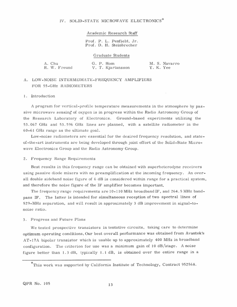
IV. ELECTRONICS "' SOLID-STATE MICROWAVE Academic Research Staff Prof. P. L. Penfield, Jr. Prof. D. H. Steinbrecher Graduate Students A. Chu R. W. Freund A. INTERMEDIATE -FREQUENCY LOW-NOISE FOR 55-GHz 1. G. P. Hom V. T. Kjartansson M. S. Navarro Y. K. Yee AMPLIFIERS RADIOMETERS Introduction A program for vertical-profile temperature measurements in the atmosphere by pas- sive microwave sensing of oxygen is in progress within the Radio Astronomy Group of the Research 53. 067 GHz Laboratory of Electronics. and 53. 596 GHz Ground-based lines are planned, experiments utilizing the with a satellite radiometer in the 60-61 GHz range as the ultimate goal. Low-noise radiometers are essential for the desired frequency resolution, and stateof-the-art instruments are being developed through joint effort of the Solid-State Microwave Electronics Group and the Radio Astronomy Group. 2. Frequency Range Requirements Best results in this frequency range can be obtained with superheterodyne receivers using passive diode mixers with no preamplification at the incoming frequency. An over- all double sideband noise figure of 6 dB is considered within range for a practical system, and therefore the noise figure of the IF amplifier becomes important. The frequency range requirements are 10-110 MHz broadband IF, pass IF. and 264.5 MHz band- The latter is intended for simultaneous reception of two spectral lines of 529-MHz separation, and will result in approximately 3 dB improvement in signal-tonoise ratio. 3. Progress and Future Plans We tested prospective transistors in tentative circuits, taking care to determine optimum operating conditions. Our best overall performance was obtained from Avantek's AT-17A bipolar transistor which is configuration. usable up to approximately 400 MHz in broadband The criterion for use was a minimum gain of 10 dB/stage. figure better than 1. 3 dB, typically 1. 1 dB, is A noise obtained over the entire range in This work was supported by California Institute of Technology, Contract 952568. QPR No. 105 a IU n TRANSFORMER: 3x6 TURNS ON 9 mm DIAMETER 3E2A TOROID -17 A Fig. IV-1. Tentative 10-110 MHz broadband circuit. 120 K Fig. IV-2. Tentative 5-500 IMHz microstrip circuit. COLLECTOR SUPPLY 200 0 50 Q LOAD L Fig. IV-3. QPR No. 105 W\idcband 2:1 transformer. (IV. SOLID-STATE MICROWAVE ELECTRONICS) 10-110 MHz design, with more than 20 dB gain/stage. Under optimal conditions for a single frequency, less than 1 dB (0. 85 dB) noise figure has been repeatedly measured at 60 MHz. A tentative microstrip circuit gives a 1. 6 dB noise figure at 250 MHz, and 1. 9 dB at 500 MHz. Little attention has been paid to frequency-response flatness, thus far. We are now making s-parameter measurements aimed at computer simulation, using MARTHA, a special circuit analysis program implemented on APL facilities. It is likely that two final versions will be built, one optimized for the 10-110 MHz range, and the other for the 250-MItz range. 4. Tentative Preamplifier Circuits a. 10-110 MHz Circuit Figure IV-1 shows the basic circuit that has been used. The output transformer is a trifiliar-wound transmission line type of transformer, providing a 200-P load impedance for the collector. The resulting gain is 28 dB at 10 MHz, falling to 24 dB at 110 MHz, in a 50 -Q system with 12 V supply voltage. b. Microstrip Circuit The microstrip circuit is shown in Fig. IV-2. The 100-2 transmission line adds inductance to the collector load impedance as the frequency increases, giving a shunt compensation peak around 350 M1Iz. Another version, using two 100- 2 transmission lines in series/parallel, in order to raise the collector load impedance to 200 2, gives higher low-frequency gain (25 dB instead of 21 dB) but falls to 10 dB at 400 MHz rather than 500 MHz as in the circuit shown in Fig. IV-1. The 2:1 transformer is shown schematically in Fig. IV-3. range than the one used in the It has a wider frequency 10-110 MHz circuit because characteristic matching is employed throughout. impedance A single unit can be used from below 1 MHz to well above 1 GHz. The ferrite beads are necessary to suppress common mode currents on the floated line, thereby permitting the two ends of the outer conductor to be connected to points of different voltage, regardless of line length relative to wavelength. The dc blocking employed permits feeding the dc bias to the collector at a point of zero signal voltage. V. T. Kjartansson References 1. P. Penfield, Jr., 1971). QPR No. 105 MARTHA User's Manual (The M.I. T. Press, Cambridge, Mass.,

