I. I
advertisement

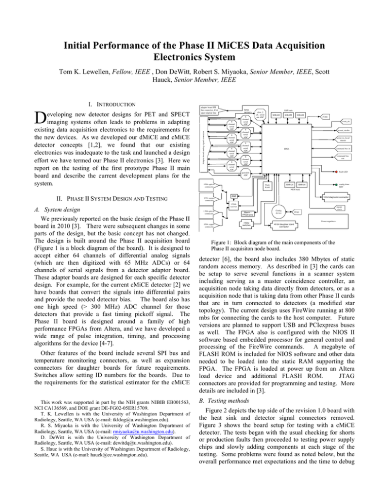
Initial Performance of the Phase II MiCES Data Acquisition Electronics System Tom K. Lewellen, Fellow, IEEE , Don DeWitt, Robert S. Miyaoka, Senior Member, IEEE, Scott Hauck, Senior Member, IEEE D eveloping new detector designs for PET and SPECT imaging systems often leads to problems in adapting existing data acquisition electronics to the requirements for the new devices. As we developed our dMiCE and cMiCE detector concepts [1,2], we found that our existing electronics was inadequate to the task and launched a design effort we have termed our Phase II electronics [3]. Here we report on the testing of the first prototype Phase II main board and describe the current development plans for the system. adapter board SPI bus connector, 4 bit spare digitial line temp sensors 8 channel serial ADC Adapter board analog signal connector I. INTRODUCTION 8 channel serial ADC 8 channel serial ADC 8 channel serial ADC 8 channel serial ADC SBP bank slow, 2 ch. serial out ADC SDRAM SDRAM SDRAM JTAG event_ok 8 channel serial ADC event_strobe serial_to_local master 8 channel serial ADC command bus in FPGA 8 channel serial ADC command bus out parrallel ADC Fault LED 1394 optical connector SDRAM Flash RAM config done LED SDRAM NIOS bank II. PHASE II SYSTEM DESIGN AND TESTING A. System design We previously reported on the basic design of the Phase II board in 2010 [3]. There were subsequent changes in some parts of the design, but the basic concept has not changed. The design is built around the Phase II acquisition board (Figure 1 is a block diagram of the board). It is designed to accept either 64 channels of differential analog signals (which are then digitized with 65 MHz ADCs) or 64 channels of serial signals from a detector adaptor board. These adapter boards are designed for each specific detector design. For example, for the current cMiCE detector [2] we have boards that convert the signals into differential pairs and provide the needed detector bias. The board also has one high speed (> 300 MHz) ADC channel for those detectors that provide a fast timing pickoff signal. The Phase II board is designed around a family of high performance FPGAs from Altera, and we have developed a wide range of pulse integration, timing, and processing algorithms for the device [4-7]. Other features of the board include several SPI bus and temperature monitoring connectors, as well as expansion connectors for daughter boards for future requirements. Switches allow setting ID numbers for the boards. Due to the requirements for the statistical estimator for the cMiCE This work was supported in part by the NIH grants NIBIB EB001563, NCI CA136569, and DOE grant DE-FG02-05ER15709. T. K. Lewellen is with the University of Washington Department of Radiology, Seattle, WA USA (e-mail: tkldog@u.washington.edu). R. S. Miyaoka is with the University of Washington Department of Radiology, Seattle, WA USA (e-mail: rmiyaoka@u.washington.edu). D. DeWitt is with the University of Washington Department of Radiology, Seattle, WA USA (e-mail: dewitdq@u.washington.edu). S. Hauc is with the University of Washington Department of Radiology, Seattle, WA USA (e-mail: hauck@ee.washington.edu). 1394 copper connector osc 10 bit diagnostic connector 1394b xceiver 1394 optical connector 1394 copper connector Maxim FPGA temp rotary switches Config device master clock JTAG Power regulators 40 bit daughter board connector Figure 1: Block diagram of the main components of the Phase II acquisiton node board. detector [6], the board also includes 380 Mbytes of static random access memory. As described in [3] the cards can be setup to serve several functions in a scanner system including serving as a master coincidence controller, an acquisition node taking data directly from detectors, or as a acquisition node that is taking data from other Phase II cards that are in turn connected to detectors (a modified star topology). The current design uses FireWire running at 800 mbs for connecting the cards to the host computer. Future versions are planned to support USB and PCIexpress buses as well. The FPGA also is configured with the NIOS II software based embedded processor for general control and processing of the FireWire commands. A megabyte of FLASH ROM is included for NIOS software and other data needed to be loaded into the static RAM supporting the FPGA. The FPGA is loaded at power up from an Altera load device and additional FLASH ROM. JTAG connectors are provided for programming and testing. More details are included in [3]. B. Testing methods Figure 2 depicts the top side of the revision 1.0 board with the heat sink and detector signal connectors removed. Figure 3 shows the board setup for testing with a cMiCE detector. The tests began with the usual checking for shorts or production faults then proceeded to testing power supply chips and slowly adding components at each stage of the testing. Some problems were found as noted below, but the overall performance met expectations and the time to debug Figure 2: Top of the Phase II electronics board showing the FPGA, half of the memories and ADCs (the other memories and ADCs are on the bottom side of the card). Figure 4: Example of a single event from a cMiCE detector with a 64 channel PMT using the prototype cMiCE adapter board (not the new boards shown in Figure 3)showing all 64 spectra and an enlargement of the anode with the largest signal. of the first tests done with signals form a cMiCE PMT based detector. A single event is show with the digitized outputs from each of the 64 anodes (the grid of small plots) and a zoomed plot of the anode with the largest signal. III. DISCUSSION AND CONCLUSION Figure 3: Phase II board connected to a cMiCE detector with new adapter cMiCE adapter boards . the card was less than we had anticipated. Once all of the components were confirmed to be operating properly, simple Verilog code was written and combined with C code in the NIOS II soft embedded processor to begin testing the card with real data. For these first tests, a prototype detector adapter board was fabricated to provide amplification and conversion of signals to differential pairs from a cMiCE detector utilizing a 64 channel Hamamatsu H8500 PMT. This setup allowed testing of the revision 1.0 Phase II board by recording event by event data digitized from all 64 analog inputs. B. Results All devices on the first prototype (revision 1.0) boards are functioning as expected after several problems were found. Modifications that were made to the board (and incorporated in the revision 1.1 board design) included: 1. FPGA pullup on pins was not adequate for some of the connections and pull up resistors were added. 2. Some clock pins in the FPGA did not have internal termination (as claimed in the specifications) and additional termination has been added. 3. Data sheet errors for the FLASH ROM and one of the power supplies led to connections that disabled the chips. The incorrectly defined pin assignments were determined and fixed 4. Other improvements in signal routing. All of the ADCs are operating at the designed sampling rates and the other support devices (e.g., Firewire transceiver, SPI bus connections, temperature sensor circuits, etc.) are working as expected. Figure 4 depicts one Testing of the Phase II board is continuing with a new adapter board for the cMiCE detectors and integration of the new FPGA Verilog code for pulse integration with pulse pile-up correction [4] as well as the timing algorithms [7] and cMiCE statistical position estimator FPGA code [6]. By the time of the MIC conference, we will have a wide range of performance results from cMiCE detectors, including examples of count rate performance, timing accuracy, and position estimation with the Phase II board. The revision 1.1 board will be ready for testing by the middle of June as well as system integration as we port over the FireWire command and control code from the MiCES scanner [3] for use with the Phase II board. REFERENCES [1] Champley, K.M., Lewellen, T.K., MacDonald, L.R., Miyaoka, R.S., Kinahan, P.E.: “Statistical LOR Estimation for High-Resolution dMiCE PET Detector”, Phys. Med. Bio. 54, pp. 6369-6382 (2009). [2] Li, X., Hunter, W.C.J., Lewellen, T.K., Miyaoka, R.S.: “Spatial Resolution Performance Evaluation for a Monolithic Cyrstal PET Detector with Cramer-Rao Lower Bound”, IEEE Nuclear Science Symposium and Medical Imaging Conference (2010). [3] Lewellen, T.K., Miyaoka, R.S., MacDonald, L.R., Haselman, M., DeWitt, D., Hauck, S.: “Evolution of the Design of a Second Generation Firewrie Based Data Acquisition System”, IEEE Nuclear Science Symposium and Medical Imaging Conference (2010). [4] Hasleman, M.D., Hauck, S., Lewellen, T.K., Miyaoka, R.S.: “FPGA-Based Pulse Pileup Correction”, IEEE Nuclear Science Symposium and Medical Imaging Conference (2010). [5] Haselman, M., Hauck, S., Lewellen, T.K., Miyaoka, R.S.: “FPGA-Based Pulse Parameter Discovery for Positron Emission Tomography”, IEEE Nuccear Science Symposium and Medical Imaging Conference pp. 2956-2961 (2009). [6] Johnson-Williams, N.G., Miyaoka, R.S., Xiaoli, L., Lewellen, T.K., Hauck, S.: “Design of a real time FPGA-based three dimensional positioning algorithm”, Nuclear Science Symposium Conference Record (NSS/MIC), 2009 IEEE pp. 3652-3659 (2009). [7] Haselman, M.D., Hauck, S., Lewellen, T.K., Miyaoka, R.S.: “Simulation of algorithms for pulse timing in FPGAs”, IEEE Nuclear Science Symposium and Medical Imaging Conference 4, pp. 3161-3165 (2007).


