CHARGE STORAGE EFFECT IN A TRILAYER STRUCTURE COMPRISING GERMANIUM NANOCRYSTALS
advertisement
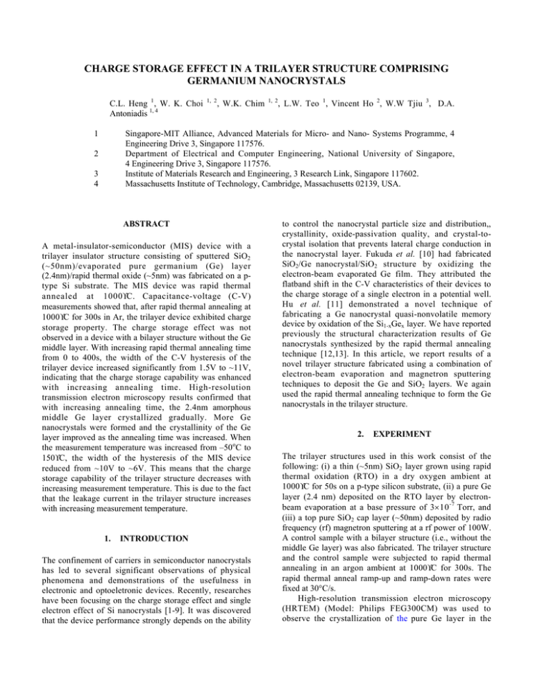
CHARGE STORAGE EFFECT IN A TRILAYER STRUCTURE COMPRISING GERMANIUM NANOCRYSTALS C.L. Heng 1 , W. K. Choi Antoniadis 1, 4 1 1, 2 , W.K. Chim 1, 2 , L.W. Teo 1, Vincent Ho 2, W.W Tjiu 3, D.A. Singapore-MIT Alliance, Advanced Materials for Micro- and Nano- Systems Programme, 4 Engineering Drive 3, Singapore 117576. Department of Electrical and Computer Engineering, National University of Singapore, 4 Engineering Drive 3, Singapore 117576. Institute of Materials Research and Engineering, 3 Research Link, Singapore 117602. Massachusetts Institute of Technology, Cambridge, Massachusetts 02139, USA. 2 3 4 ABSTRACT A metal-insulator-semiconductor (MIS) device with a trilayer insulator structure consisting of sputtered SiO2 (~50nm)/evaporated pure germanium (Ge) layer (2.4nm)/rapid thermal oxide (~5nm) was fabricated on a ptype Si substrate. The MIS device was rapid thermal annealed at 1000°C. Capacitance-voltage (C-V) measurements showed that, after rapid thermal annealing at 1000°C for 300s in Ar, the trilayer device exhibited charge storage property. The charge storage effect was not observed in a device with a bilayer structure without the Ge middle layer. With increasing rapid thermal annealing time from 0 to 400s, the width of the C-V hysteresis of the trilayer device increased significantly from 1.5V to ~11V, indicating that the charge storage capability was enhanced with increasing annealing time. High-resolution transmission electron microscopy results confirmed that with increasing annealing time, the 2.4nm amorphous middle Ge layer crystallized gradually. More Ge nanocrystals were formed and the crystallinity of the Ge layer improved as the annealing time was increased. When the measurement temperature was increased from –50oC to 150°C, the width of the hysteresis of the MIS device reduced from ~10V to ~6V. This means that the charge storage capability of the trilayer structure decreases with increasing measurement temperature. This is due to the fact that the leakage current in the trilayer structure increases with increasing measurement temperature. 1. INTRODUCTION The confinement of carriers in semiconductor nanocrystals has led to several significant observations of physical phenomena and demonstrations of the usefulness in electronic and optoeletronic devices. Recently, researches have been focusing on the charge storage effect and single electron effect of Si nanocrystals [1-9]. It was discovered that the device performance strongly depends on the ability to control the nanocrystal particle size and distribution,, crystallinity, oxide-passivation quality, and crystal-tocrystal isolation that prevents lateral charge conduction in the nanocrystal layer. Fukuda et al. [10] had fabricated SiO2/Ge nanocrystal/SiO2 structure by oxidizing the electron-beam evaporated Ge film. They attributed the flatband shift in the C-V characteristics of their devices to the charge storage of a single electron in a potential well. Hu et al. [11] demonstrated a novel technique of fabricating a Ge nanocrystal quasi-nonvolatile memory device by oxidation of the Si1-xGex layer. We have reported previously the structural characterization results of Ge nanocrystals synthesized by the rapid thermal annealing technique [12,13]. In this article, we report results of a novel trilayer structure fabricated using a combination of electron-beam evaporation and magnetron sputtering techniques to deposit the Ge and SiO2 layers. We again used the rapid thermal annealing technique to form the Ge nanocrystals in the trilayer structure. 2. EXPERIMENT The trilayer structures used in this work consist of the following: (i) a thin (~5nm) SiO2 layer grown using rapid thermal oxidation (RTO) in a dry oxygen ambient at 1000°C for 50s on a p-type silicon substrate, (ii) a pure Ge layer (2.4 nm) deposited on the RTO layer by electronbeam evaporation at a base pressure of 3×10 -7 Torr, and (iii) a top pure SiO2 cap layer (~50nm) deposited by radio frequency (rf) magnetron sputtering at a rf power of 100W. A control sample with a bilayer structure (i.e., without the middle Ge layer) was also fabricated. The trilayer structure and the control sample were subjected to rapid thermal annealing in an argon ambient at 1000°C for 300s. The rapid thermal anneal ramp-up and ramp-down rates were fixed at 30°C/s. High-resolution transmission electron microscopy (HRTEM) (Model: Philips FEG300CM) was used to observe the crystallization of the pure Ge layer in the 3. RESULTS AND DISCUSSIONS Figure 1 shows the C-V characteristics of a trilayer device (device A) and a control bilayer sample (device B) that had been rapid thermal annealed at 1000oC for 300s. It can be seen from Figure 1 that: (i) both devices A and B have a counter-clockwise hysteresis, (ii) the width of C-V hysteresis of device A is about 10V, and (iii) device B shows very small hysteresis. The results of Figure 1 indicate that the middle Ge layer plays an important role in the charge storage property of the trilayer structure. 1.80E-011 fact that the dielectric constant of the film decreases with increasing annealing time due to the precipitation of Ge nanocrystals, or the increase in the oxide thickness by oxidation of the underlying Si substrate with increasing annealing duration. Rapid annealing time: Seconds 2.00E-011 Capacitance (F) trilayer structure. The C-V measurements were carried out using a HP4284A precision LCR meter. as-prepared 10 50 100 200 400 1.60E-011 1.20E-011 8.00E-012 4.00E-012 o 1000C rapid thermal annealing Capacitance (F) 1.60E-011 device A device B 1.40E-011 -16 -12 -8 -4 0 4 8 12 16 Applied Voltage (V) 1.20E-011 1.00E-011 Figure 2: C-V curves, showing different amounts of hysteresis, of trilayer structures with a 2.4nm Ge layer that were rapid thermal annealed for duration of 0, 10, 50, 100, 200 and 400s in argon. 8.00E-012 6.00E-012 4.00E-012 2.00E-012 -16 -12 -8 -4 0 4 8 12 16 Applied voltage (V) Figure 1: C-V curves of the trilayer structure (device A) and the control bilayer structure (device B). Both devices were rapid thermal annealed at 1000oC for 300s in argon. We studied further how the charge storage capability of the trilayer structure changes with rapid thermal annealing time. Figure 2 shows the C-V curves of trilayer samples that were rapid thermal annealed for 0, 10, 50, 100, 200 and 400s, respectively. It can be seen that the hysterisis of the C-V curves for the as-prepared sample is very small (1.5V). However, after 10s of rapid thermal annealing, the width of the hysterisis increases to ~7V. This means that the trilayer structure exhibits charge-storage capability after 10s annealing. With increasing annealing time up to 400s, the width of the C-V hysterisis widen to ~11V. Note that the C-V curve shifts slightly to the left and the maximum capacitance of the C-V curves decreases from 18.5 to 14 pF with increasing annealing duration. We suggest that more Ge nanocrystals were formed with increasing annealing time. The increase in the Ge nanocrystals resulted in more charges being trapped. This accounts for the widening of the C-V hysterisis and the shifting of the C-V curve to the left. The reduction in the maximum capacitance of samples prepared with increasing annealing time may be due to the The effect of annealing time on the charge storage capability of the trilayer structure was also studied using the HRTEM. Figures 3(a), 3(b) and 3(c) show the crosssectional HRTEM micrographs of the trilayer structures that were rapid thermal annealed at 1000oC for 0, 10 and 300s, respectively. Figure 3(a) shows that the as-prepared trilayer structure has distinguishable interfaces between the middle Ge layer with the RTO and top cap oxide layers, and that the Ge layer is amorphous. After rapid thermal annealing for 10s (see Figure 3(b)), the interfaces become less obvious and the Ge middle layer begins to shrink to form Ge nanocrystals. The number of Ge nanocrystals, however, is small and the lattice fringes are not very clear. This shows that the crystallinity of the Ge nanocrystals is not good. After rapid thermal annealing for 300s (Figure 3(c)), the Ge layer has shrunk to form Ge nanocrystals entirely embedded in the oxide. The size of the Ge nanocrystals is around 5nm. The distribution of the nanocrystals is nearly uniform. The density of the nanocrystals is estimated to be ~9×1011cm-2 by counting the numbers of nanocrystals from the plan-view TEM pictures directly (not shown here). The TEM observation also shows that most of the nanocrystals in Figure 3(c) are single crystals, as the lattice fringes can be clearly identified. This indicates that the nanocrystals has good crystallinity after annealing for 300s. temperature and/or the increase in the thermal energy as compared to the Coulomb charging energy. o Measure temperature:C Capacitance (F) 1.60E-011 -50 -25 25 50 100 150 1.20E-011 8.00E-012 4.00E-012 0.00E+000 -16 -12 -8 -4 0 4 8 12 16 Applied Voltage (V) Figure 4: C-V curves measured at temperatures of –50, -25, 25, 50, 100 and 150oC, respectively, of the trilayer structure. 4. CONCLUSION In conclusion, we have demonstrated a novel trilayer structure device comprising of Ge nanocrystals that has potential in memory applications. The Ge nanocrystals embedded in the oxide is formed by electron-beam evaporation of a thin 2.4nm Ge layer as the middle layer of a trilayer structure. The charge storage capability was improved significantly with increasing annealing time from 10s to 400s, but decreased gradually with increasing measurement temperature from –50oC to 150oC. Figure 3: (a), (b) and (c) show the cross-sectional HRTEM images of trilayer structures that were rapid thermal annealed at 1000oC for 0, 10 and 300s, respectively. In order to investigate the charge storage capability of device A at different temperatures, we measure the width of the C-V hysteresis from –50oC to 150oC, and the results are shown in Figure 4. It can be seen that at –50oC, the hysterisis loop is very large. This means that the charge storage capability is at its best. With increasing measuring temperature from –50 to 150oC, the width of the C-V hysteresis reduces gradually from 10V to 6V and the slope of the C-V curve for the charging branch (sweep from negative to positive gate voltage) becomes gentler. The hysteresis becomes very small at 200oC and this indicates that the device loses its charge-storage capability entirely. The reduction in the hysteresis may be related to the increasing leakage current with increasing measurement ACKNOWLEDGEMENT The authors would like to thank the Singapore-MIT Alliance for financial support for this project. REFERENCES 1 . S. Tiwari, F. Rana, H. Hanafi, A. Hartstein, E.F. Crabbe, and K. Chan, Appl. Phys. Lett. 68, 1377 (1996). 2. S. Tiwari, F. Rana, K. Chan, L. Shi, and H. Hanafi, Appl. Phys. Lett. 69, 1232 (1996). 3. Y. Shi, K. Saito, H. Ishika, and T. Hiramoto, Jpn. J. Appl. Phys. 38, 2453 (1998). 4. S.H. Choi and R.G. Elliman, Appl. Phys. Lett. 75, 968 (1999). 5 . E. Kapetanakis, P. Normand, and D. Tsoukalas, K. Beltsios, J. Stoemenos, S.Zhang and J. van den Berg, Appl. Phys. Lett. 77, 3450 (2000). 6. H. Kim, S. Han, K. Han, J. Lee, and H. Shin, Jpn. J. Appl. Phys. 40, 447 (2000). 7. M. L. Ostraat, J.W. De Blauwe and M.L. Green, L.D. Bell, M.L. Brongersma, J. Casperson, R.C. Flagan, and H.A. Atwater, Appl. Phys. Lett. 79, 433 (2001). 8 . A. Thean and J.P. Leburton, IEEE Electron Device Lett. 23, 148 (2001). 9. A. Dutta, Y. Hayafune, and S. Oda, Jpn. J. Appl. Phys. 39, L855 (2000). 10. T. Kobayashi, T. Endoh, H. Fukuda, S. Nomura, A. Sakai and Y. Ueda, Appl. Phys. Lett. 71, 1195 (1997). 11. Y.C. King, T.J. King, and C. Hu, IEEE Trans. Electron Devices 48, 696 (2001). 12. W.K. Choi, V. Ng, S.P. Ng, H.H. Thio, Z.X. Shen, and W.S. Li, J. Appl. Phys. 86, 1398 (1999). 13. W.K. Choi, Y.W. Ho, S.P. Ng, and V. Ng, J. Appl. Phys. 89, 2168 (2001).
