CMU 18-447 Introduction to Computer Architecture, Spring 2015
advertisement
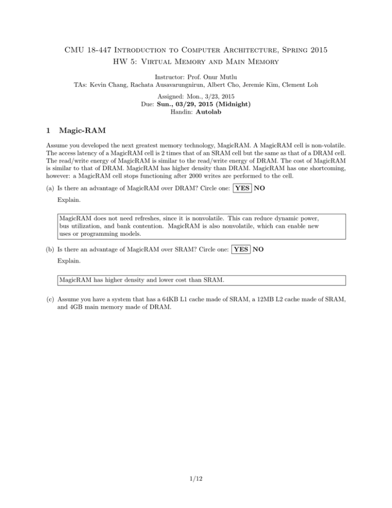
CMU 18-447 Introduction to Computer Architecture, Spring 2015 HW 5: Virtual Memory and Main Memory Instructor: Prof. Onur Mutlu TAs: Kevin Chang, Rachata Ausavarungnirun, Albert Cho, Jeremie Kim, Clement Loh Assigned: Mon., 3/23, 2015 Due: Sun., 03/29, 2015 (Midnight) Handin: Autolab 1 Magic-RAM Assume you developed the next greatest memory technology, MagicRAM. A MagicRAM cell is non-volatile. The access latency of a MagicRAM cell is 2 times that of an SRAM cell but the same as that of a DRAM cell. The read/write energy of MagicRAM is similar to the read/write energy of DRAM. The cost of MagicRAM is similar to that of DRAM. MagicRAM has higher density than DRAM. MagicRAM has one shortcoming, however: a MagicRAM cell stops functioning after 2000 writes are performed to the cell. (a) Is there an advantage of MagicRAM over DRAM? Circle one: YES NO Explain. MagicRAM does not need refreshes, since it is nonvolatile. This can reduce dynamic power, bus utilization, and bank contention. MagicRAM is also nonvolatile, which can enable new uses or programming models. (b) Is there an advantage of MagicRAM over SRAM? Circle one: YES NO Explain. MagicRAM has higher density and lower cost than SRAM. (c) Assume you have a system that has a 64KB L1 cache made of SRAM, a 12MB L2 cache made of SRAM, and 4GB main memory made of DRAM. 1/12 Assume you have complete design freedom and add structures to overcome the shortcoming of MagicRAM. You will be able to propose a way to reduce/overcome the shortcoming of MagicRAM (note that you can design the hierarchy in any way you like, but cannot change MagicRAM itself). Does it makes sense to add MagicRAM anywhere in this memory hierarchy given that you can potentially reduce its shortcoming? Circle one: YES NO If so, where would you place MagicRAM? Depict in the figure above clearly and describe why you made this choice. Many answers are possible. One option: Place MagicRAM below DRAM in the hierarchy, and use DRAM as a cache to MagicRAM. This way, DRAM performs write coalescing so that MagicRAM does not wear out as quickly. Another option could be to place MagicRAM “next to” DRAM (on the same or another channel), and use MagicRAM explicitly for read-only data. If not, why not? Explain below clearly and methodically. 2/12 (d) Propose a way to reduce/overcome the shortcoming of MagicRAM by modifying the given memory hierarchy. Be clear in your explanations and illustrate with drawings to aid understanding. Explanation: A write-combining/coalescing buffer could be added. The memory hierarchy could also perform wear-leveling, or it could predict which data is less likely to be modified and place only that data in MagicRAM. Figure(s): 3/12 2 Memory Scheduling Row-Buffer Conflicts. The following timing diagram shows the operation of a single DRAM channel and a single DRAM bank for two back-to-back reads that conflict in the row-buffer. Immediately after the bank has been busy for 10ns with a READ, data starts to be transferred over the data bus for 5ns. 10ns Bank 10ns PRECHARGE 10ns 10ns ACTIVATE READ 10ns PRECHARGE 10ns ACTIVATE READ 1ns 1ns 1ns 1ns 1ns 1ns 1ns 1ns 1ns 1ns 1ns 1ns time Command Bus time Address Bus time Data Bus 5ns 5ns 64B 64B time (a) Given a long sequence of back-to-back reads that always conflict in the row-buffer, what is the data throughput of the main memory system? Please state your answer in gigabytes/second. 64B/30ns = 32B/15ns = 32GB/15s = 2.13GB/s (b) To increase the data throughput, the main memory designer is considering adding more DRAM banks to the single DRAM channel. Given a long sequence of back-to-back reads to all banks that always conflict in the row-buffers, what is the minimum number of banks that is required to achieve the maximum data throughput of the main memory system? 30ns/5ns = 6 Row-Buffer Hits. The following timing diagram shows the operation of the single DRAM channel and the single DRAM bank for four back-to-back reads that hit in the row-buffer. It is important to note that rowbuffer hits to the same DRAM bank are pipelined: while each READ keeps the DRAM bank busy for 10ns, up 4/12 to at most half of this latency (5ns) can be overlapped with another read that hits in the row-buffer. (Note that this is different from Lab 6 where we unrealistically assumed that row-buffer hits are non-pipelined.) READ READ Bank time READ READ 1ns 1ns 1ns 1ns 1ns 1ns 1ns 1ns Command Bus time Address Bus time Data Bus 5ns 5ns 5ns 5ns 64B 64B 64B 64B time (c) Given a long sequence of back-to-back reads that always hits in the row-buffer, what is the data throughput of the main memory system? Please state your answer in gigabytes/second. 64B/5ns = 64GB/5s = 12.8GB/s (d) When the maximum data throughput is achieved for a main memory system that has a single DRAM channel and a single DRAM bank, what is the bottleneck that prevents the data throughput from becoming even larger? Circle all that apply. BANK COMMAND BUS ADDRESS BUS DATA BUS Memory Scheduling Policies. The diagram below shows the memory controller’s request queue at time 0. The shaded rectangles are read requests generated by thread T 0, whereas the unshaded rectangles are read requests generated by thread T 1. Within each rectangle, there is a pair of numbers that denotes the request’s (BankAddress, RowAddress). Assume that the memory system has a single DRAM channel and four DRAM banks. Further assume the following. • All the row-buffers are closed at time 0. • Both threads start to stall at time 0 because of memory. • A thread continues to stall until it receives the data for all of its requests. • Neither thread generates more requests. (0,0) (3,0) (2,4) (1,9) (0,7) Youngest (0,0) (0,0) (0,0) Oldest We provide two sets of answers. The correct way to solve the problem is to model contention in the banks as well as in all of the buses (address/command/data). This answer is what immediately follows. However, no student modeled it to this level of detail. Therefore, we decided to give full credit if you modeled contention in only the banks correctly. This answer is given in the answer boxes. For extra credits (15 points), please make sure that you model contention in the banks as well as in all of the buses (address/command/data). 5/12 (e) For the FCFS scheduling policy, calculate the memory stall time of T 0 and T 1. 10 20 RD ACT Bank 0 10ns RD 5ns 30 RD 40 PRE 5ns 50 ACT 10ns 10ns 60 RD 70 PRE 10ns 10ns 80 ACT RD ACT 10ns 10ns RD Bank 1 10ns ACT RD Bank 2 5ns ACT Bank 3 RD 5ns 3ns T0: (10 + 5 + 5 + 10 + 10 + 10) + 10 + 10 + 10 + 10 + 5 = 95ns T1: (10 + 5 + 5 + 10 + 10 + 10) + 1 + 10 + 5 + 5 + 10 + 5 = 86ns (f) For the FR-FCFS scheduling policy, calculate the memory stall time of T 0 and T 1. 10 20 RD ACT Bank 0 10ns RD 5ns 30 40 RD RD 5ns 60 PRE 10ns ACT 70 ACT 10ns 80 RD 10ns RD Bank 1 5ns ACT RD Bank 2 5ns ACT Bank 3 50 RD 3ns 5ns 5ns T0: (10 + 5 + 5 + 5 + 5 + 5 + 5) + 10 + 5 = 55ns T1: (10 + 5 + 5 + 5 + 5 + 5 + 5) + 10 + 10 + 10 + 10 + 5 = 85ns (g) For the PAR-BS scheduling policy, calculate the memory stall time of T 0 and T 1. Assume that all eight requests are included in the same batch. 10 ACT Bank 0 20 RD 30 PRE 10ns 10ns RD ACT RD 5ns ACT 3ns RD 5ns 5ns Bank 2 Bank 3 50 RD ACT 10ns ACT Bank 1 40 RD 5ns T0: (10 + 5 + 5) + 1 + 10 + 10 + 5 + 5 + 5 + 10 + 5 = 71ns T1: (10 + 5 + 5) + 5 + 10 + 5 = 40ns 6/12 60 RD 5ns RD 5ns 70 80 (e) For the FCFS scheduling policy, calculate the memory stall time of T 0 and T 1. Bank 0 is the critical path for both threads. T 0: T 1: T0 = Closed + Pipelined-Hit + Pipelined-Hit + Conflict + Conflict + Data = (ACT+RD)+(RD/2)+(RD/2)+(PRE+ACT+RD)+(PRE+ACT+RD)+DATA = 20ns + 5ns + 5ns + 30ns + 30ns + 5ns = 95ns T1 = Closed + Pipelined-Hit + Pipelined-Hit + Conflict + Data = (ACT+RD)+(RD/2)+(RD/2)+(PRE+ACT+RD)+DATA = 20ns + 5ns + 5ns + 30ns + 5ns = 65ns (f) For the FR-FCFS scheduling policy, calculate the memory stall time of T 0 and T 1. Bank 0 is the critical path for both threads. First, we serve all four shaded requests since they are row-buffer hits. Lastly, we serve the unshaded request. T 0: T 1: T0 = Closed + Pipelined-Hit + Pipelined-Hit + Pipelined-Hit + Data = (ACT+RD)+(RD/2)+(RD/2)+(RD/2)+DATA = 20ns + 5ns + 5ns + 5ns + 5ns = 40ns T1 = Closed + Pipelined-Hit + Pipelined-Hit + Pipelined-Hit + Conflict + Data = (ACT+RD)+(RD/2)+(RD/2)+(RD/2)+(PRE+ACT+RD)+DATA = 20ns + 5ns + 5ns + 5ns + 30ns + 5ns = 70ns (g) For the PAR-BS scheduling policy, calculate the memory stall time of T 0 and T 1. Assume that all eight requests are included in the same batch. 7/12 First, we serve all four unshaded requests in parallel across the four banks. Then, we serve all four shaded requests in serial. T 0: T 1: T0 = Closed + Conflict + Pipelined-Hit + Pipelined-Hit + Pipelined-Hit + Data = (ACT+RD)+(PRE+ACT+RD)+(RD/2)+(RD/2)+(RD/2)+DATA = 20ns + 30ns + 5ns + 5ns + 5ns + 5ns = 70ns T1 = Closed + Data = (ACT+RD)+DATA = 20ns + 5ns = 25ns 8/12 3 Cache and Virtual Memory A four-way set-associative writeback cache has a 211 · 89-bit tag store. The cache uses a custom replacement policy that requires 9 bits per set. The cache block size is 64 bytes. The cache is virtually-indexed and physically-tagged. Data from a given physical address can be present in up to eight different sets in the cache. The system uses hierarchical page tables with two levels. Each level of the page table contains 1024 entries. A page table may be larger or smaller than one page. The TLB contains 64 entries. (a) How many bits of the virtual address are used to choose a set in the cache? tag store: 89 bits = (9 replacement + 4 dirty + 4 valid) + 4 * (18 physical tag bigs) 211 → 2K sets → 8K blocks → 512KB cache 11 (b) What is the size of the cache data store? 512KB (c) How many bits in the Physical Frame Number must overlap with the set index bits in the virtual address? 3 (d) On the following blank figure representing a virtual address, draw in bitfields and label bit positions for “cache block offset” and “set number.” Be complete, showing the beginning and ending bits of each field. Virtual Address: 16 Index 6 5 Block offset 0 (e) On the following blank figure representing a physical address, draw in bitfields and label bit positions for “physical frame number” and “page offset.” Be complete, showing the beginning and ending bits of each field. Physical Address: 31 PFN 14 13 Page offset (f) What is the page size? 16KB (g) What is the size of the virtual address space? 16GB (h) What is the size of the physical address space? 4GB 9/12 0 4 0x44444444 A 32-bit processor implements paging-based virtual memory using a single-level page table. The following are the assumptions about the processor’s virtual memory. • The number of bytes in a page is greater than four and is also a power of two. • The base address of the page table is page-aligned. • A page table entry (PTE) stores only the physical page number and has the following format. All of the unused bits in the PTE are set to 0. Bit 31 Bit 0 unused physical page number The following figure shows the physical memory of the processor at a particular point in time. 31 0 0xFFFFFFFF 0x44444444 0x00000044 0x44454444 0x44444444 0x00000000 4GB Physical Memory At this point, when the processor executes the following piece of code, it turns out that the processor accesses the page table entry residing at the physical address of 0x44444444. char *ptr = 0x44444444; char val = *ptr; // val == 0x44 What is the page size of the processor? Please show work for partial credit. (The answer box is continued on the next page.) Let n be equal to log2 (pagesize). • • • • • Virtual Address (VA) = 0x44444444 Virtual Page Number (VPN) = VA >> n Physical Address Of PTE (PTE PA) = 0x44444444 Size of PTE (PTE SIZE) = 4 Page Table Base Address (PTBA) = PTE PA - VPN * PTE SIZE 10/12 Clue 1: PTBA is page-aligned. PTBA & ∼(1<<n) = 0 ∴ (PTE PA - VPN * PTE SIZE) & ∼(1<<n) = 0 ∴ (0x44444444-(0x44444444>>n)*4) & ∼(1<<n) = 0 ∴ (0x44444444-(0x44444444>>(n-2)) & ∼(1<<n) = 0 This means that n is of the form: 4k + 2, where k is an integer. Possible values of n: 6, 10, 14, 18, 22, 26, 30. For these values of n, let us check whether the following equation is indeed equal to 0. (0x44444444-(0x44444444>>(n-2)) & ∼(1<<n) n=6: n=10: n=14: n=18: n=22: n=26: n=30: (0x44444444-(0x44444444>>4)) (0x44444444-(0x44444444>>8)) (0x44444444-(0x44444444>>12)) (0x44444444-(0x44444444>>16)) (0x44444444-(0x44444444>>20)) (0x44444444-(0x44444444>>24)) (0x44444444-(0x44444444>>28)) & & & & & & & ∼(1<<6) ∼(1<<10) ∼(1<<14) ∼(1<<18) ∼(1<<22) ∼(1<<26) ∼(1<<30) = = = = = = = 0x40000000 0x44000000 0x44400000 0x44440000 0x44444000 0x44444400 0x44444440 & & & & & & & 0x0000003F 0x000003FF 0x00003FFF 0x0003FFFF 0x003FFFFF 0x03FFFFFF 0x3FFFFFFF = 0 = 0 = 0 = 0 != 0 != 0 != 0 Possible values of n: 6, 10, 14, 18. Clue 2: Physical address 0x44454444 is not a PTE For the possible values of n, let us check whether the last PTE of the page table is stored at a lower physical address than 0x44454444. PA of Last PTE (LPTE PA) = PTBA + ((1<<(32-n)) - 1) * PTE SIZE ∴ LPTE PA = PTBA + ((1<<(34-n))-4) n=6: n=10: n=14: n=18: 0x40000000+((1<<28)-4) 0x44000000+((1<<24)-4) 0x44400000+((1<<20)-4) 0x44440000+((1<<16)-4) = = = = 0x40000000+0x0ffffffc 0x44000000+0x00fffffc 0x44400000+0x000ffffc 0x44440000+0x0000fffc The only possible value of n: 18. 11/12 = = = = 0x4ffffffc 0x44fffffc 0x444ffffc 0x4444fffc > > > < 0x44454444 0x44454444 0x44454444 0x44454444 5 Research Paper Summaries Please read the following handout on how to write critical reviews. We will give out extra credit that is worth 0.5% of your total grade for each good summary/review. • Lecture slides on guidelines for reviewing papers. http://www.ece.cmu.edu/˜ece447/s15/lib/exe/fetch.php?media=onur-447-s15-howto-do-the-paper-reviews.pdf (a) Write a half-page summary for the following paper: Onur Mutlu, Justin Meza, and Lavanya Subramanian, ”The Main Memory System: Challenges and Opportunities” Invited Article in Communications of the Korean Institute of Information Scientists and Engineers (KIISE), 2015. http://users.ece.cmu.edu/˜omutlu/pub/main-memory-system_kiise15.pdf (b) Extra credit (0.5% of your grade). Write a half-page summary for the following paper: Vivek Seshadri, Yoongu Kim, Chris Fallin, Donghyuk Lee, Rachata Ausavarungnirun, Gennady Pekhimenko, Yixin Luo, Onur Mutlu, Michael A. Kozuch, Phillip B. Gibbons, and Todd C. Mowry, ”RowClone: Fast and Energy-Efficient In-DRAM Bulk Data Copy and Initialization” Proceedings of the 46th International Symposium on Microarchitecture (MICRO), Davis, CA, December 2013. http://users.ece.cmu.edu/˜omutlu/pub/rowclone_micro13.pdf 12/12

