M. Meyyappan Director, Center for Nanotechnology NASA Ames Research Center
advertisement
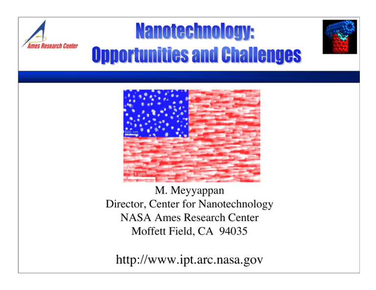
M. Meyyappan Director, Center for Nanotechnology NASA Ames Research Center Moffett Field, CA 94035 http://www.ipt.arc.nasa.gov Nanotechnology is the creation of USEFUL/FUNCTIONAL materials, devices and systems through control of matter on the nanometer length scale and exploitation of novel phenomena and properties (physical, chemical, biological) at that length scale “If I were asked for an area of science and engineering that will most likely produce the breakthroughs of tomorrow, I would point to nanoscale science and engineering.” -Neal Lane Former Assistant to the President for Science And Technology Me ltin gp oin t-1 064 °C Source: K.J. Klabunde, 2001 • Computing and Data Storage • Materials and Manufacturing • Health and Medicine • Energy and Environment • Transportation • National Security Nanotechnology is an enabling technology • Space exploration • • • Processors with declining energy use and cost per gate, thus increasing efficiency of computer by 106 • Small mass storage devices: multi-tera bit levels • Integrated nanosensors: collecting, processing and communicating massive amounts of data with minimal size, weight, and power consumption • Higher transmission frequencies and more efficient utilization of optical spectrum to provide at least 10 times the bandwidth now • Display technologies • Quantum computing *First single nanotube logic device – Inverter demonstration (Appl. Phys. Lett., Nov. 2001) V0 VDD DS Vin 2.5 V DD =2.9 V 1.5 p Vi 1.0 n n t 0 V 0.5 0.0 0.0 Vou 0.5 1.0 1.5 V in(V) 2.0 (nA) VDD DS Vout(V) 2.0 100 VDS=10 mV 80 p-MOSFET 60 40 20 0 -20 -15 -10 -5 0 Vg(V) I Vout n-type p-type Carbon nanotube (nA) by Chongwu Zhou (USC) and Jie Han (NASA Ames) 12 VDS=10 mV n-MOSFET 8 4 2.5 0 -10 -5 0 5 10 Vg (V) (Beyond the SIA Roadmap for Silicon) • Must be easier and cheaper to manufacture than CMOS • Need high current drive; should be able to drive capacitances of interconnects of any length • High level of integration (>1010 transistors/circuit) • High reproducibility (better than ± 5%) • Reliability (operating time > 10 years) • Very low cost ( < 1 µcent/transistor) • Better heat dissipation characteristics and amenable solutions • Everything about the new technology must be compelling and simultaneously further CMOS scaling must become difficult and not cost-effective. Until these two happen together, the enormous infrastructure built around silicon will keep the silicon engine humming…. • • • • Neural tree with 14 symmetric Y-junctions Branching and switching of signals at each junction similar to what happens in biological neural network Neural tree can be trained to perform complex switching and computing functions Not restricted to only electronic signals; possible to use acoustic, chemical or thermal signals Motivations for selecting Single Crystalline Nanowires & Nanowalls (in Nano-scale Electronics) High single crystallinity ⇒ Low defect density, grain boundary free ϖ Well-defined surface structural properties ⇒ Enhanced interfacial engineering Predictable electron transport properties ⇒ Predictable device performance Unique physical properties due to quantum confinement effects ⇒ Enhancement in device characteristics Tunable electronic properties by doping ⇒ Enhancement in device characteristics Truly bottom-up integration approach ⇒ Innovative fabrication schemes Potential to revolutionize nano-scale science and technology Challenges in Nanowire Growth • Uni-directional nanowire growth; vertical or horizontal substrate engineering electric field directed ⇔ ⇔ Understanding of the interfacial epitaxial relationship between potential substrates and nanowire structures ⇔ modeling and simulations ⇔ experiments ⇔ combinatorial approach (0001) Nanowire-based Vertical Surround Gate FET MWNT Interconnects ? CNT advantages: (1) Small diameter (2) High aspect ratio (3) Highly conductive along the axis (4) High mechanical strength Question: How to do this ? Bottom-up Approach for CNT Interconnects Metal Deposition Ti, Mo, Cr, Pt SiO2/Si Ni At ~ 400 to 800° C Catalyst Patterning Top Metal Layer Deposition Plasma CVD CMP TEOS CVD J. Li, Q. Ye, A. Cassell, H. T. Ng, R. Stevens, J. Han, M. Meyyappan, Appl. Phys. Lett., 82(15), 2491 (2003) • Expanding ability to characterize genetic makeup will revolutionize the specificity of diagnostics and therapeutics - Nanodevices can make gene sequencing more efficient • Effective and less expensive health care using remote and in-vivo devices • New formulations and routes for drug delivery, optimal drug usage Nanotube-based biosensor for cancer diagnostics • More durable, rejection-resistant artificial tissues and organs • Sensors for early detection and prevention • Our interest is to develop sensors for astrobiology to study origins of life. CNT, though inert, can be functionalized at the tip with a probe molecule. Current study uses AFM as an experimental platform. • The technology is also being used in collaboration with NCI to develop sensors for cancer diagnostics - Identified probe molecule that will serve as signature of leukemia cells, to be attached to CNT - Current flow due to hybridization will be through CNT electrode to an IC chip. - Prototype biosensors catheter development • • • • High specificity Direct, fast response High sensitivity Single molecule and cell signal capture and detection • Ability to synthesize nanoscale building blocks with control on size, composition etc. further assembling into larger structures with designed properties will revolutionize materials manufacturing - Manufacturing metals, ceramics, polymers, etc. at exact shapes without machining - Lighter, stronger and programmable materials - Lower failure rates and reduced life-cycle costs - Bio-inspired materials - Multifunctional, adaptive materials - Self-healing materials Self-Cleaning Surfaces: Lotus Effect 10 mm W. Barthlott, Univ. of Hamburg On a smooth surface the contaminating particles are only moved by the water droplet (left). In contrast to that, on a rough surface they stick to the droplet rolling off the leaf thus being washed off (right). Epicuticular wax (Source: Metin Sitti, CMU) • Heat shock protein (HSP 60) in organisms living at high temperatures (“extremophiles”) is of interest in astrobiology • HSP 60 can be purified from cells as a double-ring structure consisting of 16-18 subunits. The double rings can be induced to self-assemble into nanotubes. Extremophile Proteins for Nano-scale Substrate Patterning Nano-scale engineering for high resolution lithography Future: Bio-based lithography •Batch self-assembly •Evolving •Inexpensive “quantum dots” nm resolution • Energy Production - Clean, less expensive sources enabled by novel nanomaterials and processes • Energy Utilization - High efficiency and durable home and industrial lighting - Solid state lighting can reduce total electricity consumption by 10% and cut carbon emission by the equivalent of 28 million tons/year (Source: Al Romig, Sandia Lab) • Materials of construction sensing changing conditions and in response, altering their inner structure • Thermal barrier and wear resistant coatings • High strength, light weight composites for increasing fuel efficiency • High temperature sensors for ‘under the hood’ • Improved displays • Battery technology • Wear-resistant tires • Automated highways • Very high sensitivity, low power sensors for detecting chem/bio/nuclear threats • Light weight military platforms, without sacrificing functionality, safety and soldier security - Reduce fuel needs and logistical requirements • Reduce carry-on weight of soldier gear - Increased functionality per unit weight • Advanced miniaturization, a key thrust area to enable new science and exploration missions - Ultrasmall sensors, power sources, communication, navigation, and propulsion systems with very low mass, volume and power consumption are needed • Revolutions in electronics and computing will allow reconfigurable, autonomous, “thinking” spacecraft • Nanotechnology presents a whole new spectrum of opportunities to build device components and systems for entirely new space architectures - Networks of ultrasmall probes on planetary surfaces - Micro-rovers that drive, hop, fly, and burrow - Collection of microspacecraft making a variety of measurements Europa Submarine • Short term (< 5 years) - Nanoparticles * Automotive industry (body moldings,timing belts, engine covers…) * Packaging industry * Cosmetics - Flat panel displays - Coatings - CNT-based probes in semiconductor metrology - Tools - Catalysts (extension of existing market) • Medium term (5-10 years) - Memory devices Fuel cells, batteries Biosensors (CNT, molecular, qD based) Biomedical devices Advances in gene sequencing Advances in lighting • Long term (> 15 years) - Nanoelectronics (CNT) Molecular electronics Routine use of new composites in Aerospace, automotive (risk-averse industries) Many other things we haven’t even thought of yet • Lots of nanoscience now, some nice nanotechnology; more emphasis on technology development and participation from engineering communities are needed • People do not buy technology; they buy products - Robust product development is critical to realize the potential - Early and periodic wins, a must to Source: UC Berkeley keep investor confidence high • Recognition of nano-micro-macro hierarchy in product development • Need some sanity in issuing patents • Given the long term nature of the technology and payoffs in terms of job creation and economic returns, - Lack of patience from Federal Government will kill the field - But history indicates, Federal agencies have been responsible for numerous technology wins in the last 50 years - So, ignore the hype and stay the course for the long run • Venture community behavior will determine the fate - Lack of patience will hurt the startup activities - Indiscriminate investment like in the dotcom days will seal the field • Educating future generation scientists and engineers • Nanotechnology is an enabling technology that will impact electronics and computing, materials and manufacturing, energy, transportation…. • The field is interdisciplinary but everything starts with material science. Challenges include: - Novel synthesis techniques - Characterization of nanoscale properties - Large scale production of materials - Application development • Opportunities and rewards are great and hence, tremendous worldwide interest • Integration of this emerging field into engineering and science curriculum is important to prepare the future generation of scientists and engineers
