letters to nature
advertisement
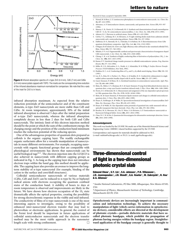
letters to nature Absorbance (arbitrary units) 0.1 0 20 40 60 80 100 Time (hours) 1 CdS 0.1 0 20 40 60 Time (min) 1 CdSe 0.1 0 0 Received 22 June; accepted 6 September 2000. 1 ZnO 0.3 0.6 50 100 150 200 Time (min) 0.9 1.2 1.5 Energy (eV) Figure 4 Infrared absorption spectra of n-type ZnO (4.4 nm), CdS (7 nm) and CdSe (5.4 nm) nanocrystals capped with TOPO. The insets are the corresponding time evolution of the infrared absorbance maximum normalized for comparison. We note that the x-axis of the inset for ZnO is in hours. infrared absorption maximum. As expected from the relative reduction potentials of the semiconductor and of the constituent elements, n-type ZnO nanocrystals are more stable than CdS and CdSe. At room temperature, approximately 30% of the initial infrared absorption is observed 5 days after the initial preparation of n-type ZnO nanocrystals, whereas the infrared absorption completely decays in less than 2 days for both CdS and CdSe nanocrystals. The intrinsic limit of this electron injection method should be the point at which the sum of the con®nement energy, the charging energy and the position of the conduction band minimum reaches the reduction potential of the reducing species. One of the advantageous properties of quantum dots prepared as colloids is the organic capping layer. The readily exchangeable organic surfactants allow for a versatile manipulation of nanocrystals in many different environments. For example, recapping nanocrystals with organic functional groups that are compatible with physiological environments has shown that nanocrystals can be useful biological tags20,21. The electron injection into the LUQCO is also achieved in nanocrystals with different capping groups as indicated in Fig. 3. As long as the capping layer does not introduce electron traps within the band gap, this method should be applicable. The capping layer also provides an avenue to improve the longterm stability of n-type nanocrystal (for example, binding of the cation to the surface and core/shell structures). Colloidal semiconductor nanocrystals of various materials (CdSe, CdS and ZnO) can be reduced to n-type by Na or biphenyl radical anions with electrons occupying the quantum con®ned states of the conduction band. A stability of hours to days at room temperature is observed and improvements are likely in the future. We have shown how electron occupation of the 1Se state dramatically affects the optical properties, creating the possibility for strong electrochromic response in the visible and mid-infrared. The conductivity of ®lms of n-type nanocrystals is one of the most interesting aspects to investigate, owing to the possibility of enhanced inter-nanocrystal electron transfer that may lead to photovoltaic or electronic applications. In general, the control of the Fermi level should be important in future applications of colloidal semiconductor nanocrystals and the electron transfer method may be the most viable approach in the nanometer length scale with strong con®nement. M NATURE | VOL 407 | 26 OCTOBER 2000 | www.nature.com 1. Nirmal, M. & Brus, L. E. Luminescence photophysics in semiconductor nanocrystals. Acc. Chem. Res. 32, 407±414 (1999). 2. Alivisatos, A. P. Semiconductor clusters, nanocrystals, and quantum dots. Science 271, 933±937 (1996). 3. Murray, C. B., Norris, D. J. & Bawendi, M. G. Synthesis and characterization of nearly monodisperse CdE (E = S, Se, Te) semiconductor nanocrystallites. J. Am. Chem. Soc. 115, 8706±8715 (1993). 4. Ashoori, R. C. Electrons in arti®cial atoms. Nature 379, 413±419 (1996). 5. Colvin, V. L., Schlamp, M. C. & Alivisatos, A. P. Light-emitting diodes made from cadmium selenide nanocrystals and a semiconducting polymer. Nature 370, 354±357 (1994). 6. Dabbousi, B. O., Bawendi, M. G., Onitsuka, O. & Rubner, M. F. Electroluminescence from CdSe quantum-dot/polymer composites. Appl. Phys. Lett. 66, 1316±1318 (1995). 7. O'Regan, B. & GraÈtzel, M. A low-cost, high-ef®ciency solar cell based on dye-sensitized colloidal TiO2 ®lms. Nature 353, 737±740 (1991). 8. Mikulec, F. V. et al. Organometallic synthesis and spectroscopic characterization of manganese-doped CdSe nanocrystals. J. Am. Chem. Soc. 122, 2532±2540 (2000). 9. Chiang, C. K. et al. Synthesis of highly conducting ®lms of derivatives of polyacetylene, CHx. J. Am. Chem. Soc. 100, 1013±1015 (1978). 10. Kamat, P. V. Interfacial charge transfer processes in colloidal semiconductor systems. Prog. Reaction Kinetics 19, 277±316 (1994). 11. Miller, R. J. D., McLendon, G. L., Nozik, A. J., Schmickler, W. & Willig, F. Surface Electron Transfer Processes (VCH Publishers, New York, 1995). 12. Haddon, R. C. et al. Conducting ®lms of C60 and C70 by alkali-metal doping. Nature 350, 320±322 (1991). 13. Lee, R. S., Kim, H. J., Fischer, J. E., Thess, A. & Smalley, R. E. Conductivity enhancement in singlewalled carbon nanotube bundles doped with K and Br. Nature 388, 255±257 (1997). 14. Guyot-Sionnest, P. & Hines, M. A. Intraband transitions in semiconductor nanocrystals. Appl. Phys. Lett. 72, 686±688 (1998). 15. Shim, M., Shilov, S. V., Braiman, M. S. & Guyot-Sionnest, P. Long-lived delocalized electron states in quantum dots: a step-scan Fourier transform infrared study. J. Phys. Chem. 104, 1494±1496 (2000). 16. Norris, D. J. & Bawendi, M. G. Measurement and assignment of the size-dependent optical spectrum in CdSe quantum dots. Phys. Rev. B 53, 16338±16346 (1996). 17. Shim, M. & Guyot-Sionnest, P. Permanent dipole moment and charges in colloidal semiconductor quantum dots. J. Chem. Phys. 111, 6955±6964 (1999). 18. Hoyer, P., Eichberger, R. & Weller, H. Spectroelectrochemical investigations of nanocrystalline ZnO ®lms. Ber. Bunsenges. Phys. Chem. 97, 630±635 (1993). 19. Hoyer, P. & Weller, H. Size-dependent redox potentials of quantized zinc oxide measured with an optically transparent thin layer electrode. Chem. Phys. Lett. 221, 379±384 (1994). 20. Bruchez, M. Jr, Moronne, M., Gin, P., Weiss, S. & Alivisatos, A. P. Semiconductor nanocrystals as ¯uorescent biological labels. Science 281, 2013±2016 (1998). 21. Chan, W. C. W. & Nie, S. Quantum dot bioconjugates for ultrasensitive nonisotopic detection. Science 281, 2016±2018 (1998). Acknowledgements This work was funded by the US NSF. We made use of the Materials Research Science and Engineering Center (MRSEC) shared facilities supported by the US NSF. Correspondence and requests for materials should be addressed to M.S. (e-mail: mshim@uchicago.edu) or P.G.S. (e-mail: pgs@uchicago.edu). ................................................................. Three-dimensional control of light in a two-dimensional photonic crystal slab Edmond Chow*, S.Y. Lin*, S.G. Johnson², P.R. Villeneuve², J.D. Joannopoulos², J.R. Wendt*, G.A. Vawter*, W. Zubrzycki*, H. Hou* & A. Alleman* * Sandia National Laboratories, PO Box 5800, Albuquerque, New Mexico 87185, USA ² Department of Physics, Massachusetts Institute of Technology, Cambridge, Massachusetts 02139, USA .............................................................................................................................................. Optoelectronic devices are increasingly important in communication and information technology. To achieve the necessary manipulation of light (which carries information in optoelectronic devices), considerable efforts are directed at the development of photonic crystalsÐperiodic dielectric materials that have socalled photonic bandgaps, which prohibit the propagation of photons having energies within the bandgap region. Straightforward application of the bandgap concept is generally thought to © 2000 Macmillan Magazines Ltd 983 letters to nature require three-dimensional (3D) photonic crystals1±5; their twodimensional (2D) counterparts con®ne light in the crystal plane6,7, but not in the perpendicular z direction, which inevitably leads to diffraction losses. Nonetheless, 2D photonic crystals still attract interest8±15 because they are potentially more amenable to fabrication by existing techniques and diffraction losses need not seriously impair utility. Here we report the fabrication of a waveguide-coupled photonic crystal slab (essentially a freestanding 2D photonic crystal) with a strong 2D bandgap at wavelengths of about 1.5 mm, yet which is capable of fully controlling light in all three dimensions. These features con®rm theoretical calculations16,17 on the possibility of achieving 3D light control using 2D bandgaps, with index guiding providing control in the third dimension, and raise the prospect of being able to realize unusual photonic-crystal devices, such as thresholdless lasers1. The photonic crystal slab consists of cylindrical holes etched through a thin GaAs slab and partially into a 1-mm-thick underlying Al0.9Ga0.1 As layer (Fig. 1). The nearest hole-to-hole spacing is a and the hole diameter is d (= 0.6a). The thickness (t) of the GaAs slab was chosen to be 0.5a to create a large photonic bandgap16. The Al0.9Ga0.1As layer was then wet oxidized to give a layer of AlxOy. The latter has a low refractive index (n < 1.5; ref. 18), which helps to con®ne light in the GaAs slab. In a periodic dielectric structure, electromagnetic waves experience a periodic scattering potential, as described by Maxwell's equations. Light is coherently scattered by this potential, much as electrons are scattered in an electronic crystal (Bragg scattering). So the language for describing electronic states in an electronic a light in light out y crystal19 Ðsuch as `crystal wavevector' (K) and `Brillouin zone'Ð may also be applied to describe photonic states in a photonic crystal. As a result of Bragg re¯ection, frequency gaps can also form; within these gaps, the photonic density of states vanishes and the propagation of light is strictly forbidden in all directions within the crystal. Figure 2 shows such a frequency dispersion (that is, q versus k) of a photonic crystal slab. Here, q and k are the frequency and the crystal wavevector associated with an electromagnetic wave, respectively. The shaded area represents the light-cone regionÐwhere leaky modes occurÐand the unshaded region shows where guided modes occur: the connected dots represent the guided modes within the slab (Fig. 2a). The light-cone boundary is identi®ed only in full 3D band-structure calculations17; its slope is determined by the refractive index of AlxOy cladding layer, and is slightly nonlinear because of the small penetration of etched holes into this layer. Although the dielectric±air interface of an individual hole would give rise to strong scattering and radiation losses, a periodic hole array causes coherent scattering, so that energy-momentum conservation rules prohibit the Bloch guided modes from coupling into air modes. Guided modes may be even (open circles in Fig. 2a) or odd (solid circles) with respect to re¯ection through the mirror plane (x±y plane in Fig. 1b) bisecting the slab and the cylinders of the 2D hole17. These even and odd states have strong similarities with respectively transverse electric (TE) and transverse magnetic (TM) states in two dimensions. For TE modes, there exists a large fundamental TE photonic bandgap at q = 0.263±0.34. There is also a higher-order TM gap at q = 0.345±0.378. Operating within these bandgaps, light can be strongly re¯ected by the 2D gaps and also index-guided vertically. This is how light can be fully controlled using a 2D photonic-crystal slab. In Fig. 2b, the dispersion for an unoxidized photonic-crystal slab is shown. Here the slope of the light cone, c/n, is set by the refractive index of the Al0.9Ga0.1As layer, n = 2.9; a higher n implies a lower light-cone boundary. Consequently, only the lowest TE and TM band are guided, and only a small photonic bandgap is expected. The use of a low-index AlxOy layer in our 2D slab structure design is essential for obtaining 2D guided modes and bandgaps. To probe the intrinsic optical properties of a photonic-crystal slab, we performed transmission measurements along G±K. Diode lasers were used as the light source. The transmitted light was split, and fed into a calibrated InGaAs photodetector for intensity measurements, and to an infrared (IR) camera for imaging. For ΓΚ b a 0.5 ΓΜ Light-cone boundary z GaAs λ ω (a/λ) 0.4 0.2 0.1 x y Figure 1 SEM images of a nanofabricated 2D photonic crystal slab. a, Top view showing an input ridge waveguide, a nine-period 2D hole array and an output waveguide. The holes are arranged in a triangular array, and the waveguides are used to facilitate light coupling. The 2D hole array section is a few rows wider than the waveguide to reduce light leakage around the side edges of photonic-crystal slab. b, A side view of the etched cylindrical holes, which have an etched depth of ,0.5 mm and side walls straight to within 58. Nanometre-scale fabrication of 2D holes is done using a combination of electron-beam lithography and reactive-ion-beam etching processes. The major crystal symmetry directions, G±K and G±M, are also shown. Scale bar, 1 mm. b λ ω (a/λ) AlGaAs 984 0.3 GaAs AlxOy 0 0.2 0.1 0 GaAs AlGaAs Γ Μ Κ Γ Figure 2 Computed dispersion of 2D photonic crystal slab structures. Here, q is expressed in units of (a/l), and k is plotted along symmetry directions, G, M(p/a) and K(1.15p/a). a, The bottom cladding layer is AlxOy, with refractive index n < 1.5. See text for discussion of the light-cone boundary and the shaded area. b, The bottom cladding layer is Al0.9Ga0.1As (n = 2.9). © 2000 Macmillan Magazines Ltd NATURE | VOL 407 | 26 OCTOBER 2000 | www.nature.com letters to nature precise optical alignment, the sample and lenses were mounted on a ®ve-axis moving stage, which has a movement precision of better than 50 nm. To obtain reliable transmittance data, the modal pro®le of the transmitted light must be carefully examined. In our experiment, Fig. 1b, the transmitted signal results from light coupling from (1) the input waveguide mode into (2) the photonic-crystal state and then back to (3) the output waveguide mode. If laser light is focused into the input waveguide and the crystal slab does not strongly scatter light, the output signal is a well-de®ned gaussian-shaped waveguide mode. But if the focus is inaccurate and the laser light is coupled, instead, into the undesired air mode or the substrate leaky mode, the output signal is typically broad and scattered in shape. The imaging camera at the output end is used to check the modal pro®le. Figure 3a (top) shows an image of TM light, l = 1,550 nm, transmitted through a nine-period 2D crystal sample (a = 460 nm). The mode is bright and well de®ned, and its intensity pro®le (dashed line, bottom) is gaussian. The same measurement was repeated with TE light (Fig. 3b). The image is not as bright, suggesting the existence of a TE gap, but its pro®le remains gaussian. The observed gaussian pro®les suggest that the output signal is a true measure of waveguide±crystal interaction. To ®nd the absolute intrinsic transmittance of a 2D crystal, a reference transmission is taken from an identical waveguide with no 2D crystal built in the middle section. By ratioing transmission signals, taken with and without a 2D crystal, absolute intrinsic transmittance is obtained. This procedure eliminates external uncertainties associated with re¯ection at waveguide±crystal interfaces and free-space-to-waveguide coupling ef®ciency. In Fig. 4 we show (®lled squares) the TM absolute transmittance along G±K versus the number of periods (N) of the hole array (a = 460 nm). The transmittance is high, (88 6 7)%, and independent of N. The high transmittance shows that TM light is wellguided within the crystal slab, as predicted by the calculation shown in Fig. 2b. The observed N-independence suggests that radiation loss is not important for our samples, as such loss would give an exponential dependence on N. The small deviation from perfect 100% transmission may be due to scattering at the waveguide± photonic crystal interface, which is independent of N. This observation con®rms the prediction that, under the light cone, light is guided in the 2D slab and vertical leakage loss is negligible. a λ = 1550 nm/ TM b For the TE input at q = 0.297, light is strongly attenuated, and also slowly converted to TM polarization. The total and TE transmitted light is plotted in Fig. 4 as open and solid circles, respectively. The TE transmittance drops exponentially from 50% at N = 1, to about 0.2% at N = 5, and eventually saturates at about 6 ´ 10-4. The observed exponential dependence shows that, at q = 0.297, the TE mode is in the photonic bandgap regime, which agrees with the prediction of Fig. 2a. As this TE mode is well below the light-cone boundary, vertical light leakage within the crystal is negligible. Thus, the observed absolute transmittance is a true measure of light attenuation in the 2D crystal slab. Light intensity is reduced ten times for every two periods it traverses in the crystal slab (or about 5 dB per period). In Fig. 5a, the measured and computed TE transmission spectrum along G±K is plotted on a semi-log scale as open dots and a solid line, respectively. The theoretical transmittance was calculated using 3D ®nite difference time-domain simulations20. The slightly larger observed bandgap, ,8%, may be due to small uncertainties in the fabricated hole size and lattice constant. In the bandgap, q < 0.27, transmittance as low as about 2 ´ 10 -4 is observed. At the lower band edge, q < 0.25, transmittance increases from 2 ´ 10 -4 to unity over a small Dq < 0.02, a rise of four orders of magnitude. The upper and lower TE band edges occur at q1 < 0.34 and q2 < 0.25, respectively, yielding a large gap-to-midgap ratio, 30%. The close agreement between theory and experiment also con®rms that light attenuation in the gap is due to photonic bandgap rejection, rather than to vertical leakage. In Fig. 5b, the measured TM transmission spectrum is plotted as solid dots on a semi-log scale. A theoretical curve (solid line) is also shown, which again agrees well with the experimental data. In the allowed band (q ranging from 0.240 to 0.300 a/l), an overall high transmission of 70±100% is observed; this indicates that light is indeed well guided within the 2D slab for both TE and TM polarizations in the allowed bands. The polarization conversion mentioned in Fig. 4 may be attributed to symmetry breaking in the 2D slab structure. In our sample, the upper cladding is essentially air, whereas the lower cladding is a 1-mm-thick AlxOy layer. This asymmetry17 introduces a weak coupling between the otherwise non-interacting TE and TM modes. At q = 0.297, while TE light is attenuated due to the TE gap, TM light is free to propagate and its intensity should remain roughly constant. Thus for small N (,3) in Fig. 4, TE light λ = 1550 nm/ TE 101 TM guided mode λ = 1550 nm ω = 0.297 Transmittance, T 100 10–1 10–2 (Total) 10–3 (TE) TE gap 10–4 Figure 3 Infrared images of the transmitted laser light, and their corresponding modal pro®les at l = 1,550 nm. The input laser light is coupled into and out of a ridge waveguide using a pair of aspheric lenses with a high numerical aperture (NA = 0.4). An infrared camera is used to image the laser output. a, The image of TM transmitted light is brighter as it belongs to a guided mode. b, The TE transmitted light is much weaker and is in the photonic bandgap spectral regime. Both TM and TE modal pro®les are gaussian-like. The horizontal lines are guides to the eye. NATURE | VOL 407 | 26 OCTOBER 2000 | www.nature.com 0 3 6 9 12 Number of periods, N 15 Figure 4 Absolute transmittance (T ) at q = 0.297 taken from a series of samples with different number of periods (N ). The transmittance for TM input is shown as ®lled squares. For TE input, transmitted light contains both TE and TM components. Both the TE (solid circles) and total (open circles) transmitted light attenuates exponentially as a function of N. See text for details. © 2000 Macmillan Magazines Ltd 985 letters to nature a TE 100 10–1 guided mode Absolute transmittance 10–2 band edge 10–3 gap 10–4 b TM 100 10–1 guided mode 10–2 10–3 0.18 0.22 0.26 band edge 0.3 0.34 0.38 9. Lin, S. Y. et al. Investigation of absolute photonic band gaps in two-dimensional dielectric structures. J. Mod. Opt. 41, 385±393 (1994). 10. Gruning, U. & Lehmann, V. Two-dimensional infrared photonic crystal based on microporous silicon. Thin Solid Films 276, 151±154 (1996). 11. Rosenberg, A. et al. Near-infrared two-dimensional photonic band gap materials. Opt. Lett. 21, 830± 832 (1996). 12. Krauss, T. F. et al. Two-dimensional photonic band gap structures operating at near-infrared wavelengths. Nature 383, 699±702 (1996). 13. Labilloy, D. et al. Quantitative measurement of transmission, re¯ection, and diffraction of twodimensional photonic band gap structures at near-infrared wavelengths. Phys. Rev. Lett. 79, 4147± 4150 (1997). 14. Benisty, H. et al. Optical and con®nement properties of two-dimensional photonic crystals. IEEE J. Light Wave Technol. 17, 2063±2077 (1999). 15. Kanskar, M. Observation of leaky slab modes in an air-bridged semiconductor waveguide with a twodimensional photonic lattice. Appl. Phys. Lett. 70, 1438±1440 (1997). 16. Villeneuve, P. R. et al. Three-dimensional photonic con®nement in photonic crystals of lowdimensional periodicity. IEE Proc. Optoelectron. 145, 384±390 (1998). 17. Johnson, S. G. et al. Guided modes in photonic crystal slabs. Phys. Rev. B 60, 5751±5758 (1999). 18. Kish, F. A. Planar native-oxide index-guiding AlGaAs/GaAs quantum well heterostructure lasers. Appl. Phys. Lett. 59, 1755±1757 (1991). 19. Kittel, C. Introduction to Solid State Physics Ch. 7, 185±189 (Wiley & Sons, New York, 1976). 20. Foresi, J. S. et al. Photonic bandgap micro-cavities in optical waveguides. Nature 390, 143±145 (1997). 21. Lin, S. Y. et al. Experimental demonstration of guiding and bending of electromagnet waves in a photonic crystal. Science 282, 274±276 (1998). 22. Johnson, S. et al. Elimination of cross talk in waveguide intersections. Opt. Lett. 23, 1855±1857 (1998). 23. Fan, S. et al. Channel drop tunneling through localized states. Phys. Rev. Lett 80, 960±963 (1998). 24. Fleming, J. G. & Lin, S. Y. Three-dimensional photonic crystal with a stop band from 1.35 to 1.95 mm. Opt. Lett. 24, 49±51 (1999). ω (a/λ ) Figure 5 Absolute transmittance (T ) as a function of q (= a/l) from 0.18 to 0.40. a, The TE transmittance spectrum covers the guided mode (,100% transmission at q = 0.24), band edge, and bandgap regions. The solid line is a theoretical curve. Here, q is varied by tuning l through three samples with different a: 400 nm (red dots), 430 nm (green dots) and 460 nm (blue dots), respectively. b, The transmittance for TM input light. The solid line is a theoretical curve. dominates and its intensity is close to that of total transmitted light. For 3 , N , 5, the converted TM intensity increases, yet TE light continues to be reduced, leading to a large difference between TE and the total transmitted light. For N . 5, TM polarization dominates the total transmitted light and its intensity remains constant as it is a guided mode. At this point, a back-conversion from TM to TE becomes signi®cant, leading to a nearly constant TE light intensity. The TE to TM ratio of about 0.05 for N . 5 is a measure of TE/TM mode conversion ef®ciency. This conversion process contributes to light leakage, and will limit the attenuating ef®ciency of a TE gap. Such leakage, however, may be eliminated through a symmetrical slab structure design. Possible applications of this work in planar photonic circuits include low-loss in-plane waveguide bends21, waveguide crossings22, and photonic tunnelling23 for wavelength division multiplexer/demultiplexer applications. We note that we have not obtained a complete 3D photonic bandgap24 owing to the light cone, and some radiation losses are inevitable when the structure deviates from perfect periodicityÐfor example, when boundary effects, fabrication defects, and resonant cavities23 are considered. Further work will therefore be required to minimize radiation losses in the above applications, aided by theoretical and numerical evidence that lowloss defects and cavities are possible in these structures17. M Received 19 January; accepted 24 August 2000. 1. Yablonovitch, E. Photonic band-gap structures. J. Opt. Soc. Am. B 10, 283±295 (1993). 2. John, S. Localization of light. Phys. Today 44(3), 32±40 (May 1991). 3. Ho, K. et al. Photonic band gaps in three dimensions: new layer-by-layer periodic structures. Solid State Commun. 89, 413±416 (1994). 4. Ozbay, E. et al. Measurement of three-dimensional photonic band gap in a crystal structure made of dielectric rods. Phys. Rev. B 50, 1945±1948 (1994). 5. Lin, S. Y. et al. A three-dimensional photonic crystal operating at infrared wavelengths. Nature 394, 251±253 (1998). 6. Soukoulis, C. M. (ed.) Photonic Band Gaps and Localization (NATO ASI Series B, Physics Vol. 308, Plenum, New York, 1993). 7. Joannoupoulos, J., Meade, R. & Winn, J. Photonic Crystals (Princeton, New York, 1995). 8. Robertson, W. M. et al. Measurement of photonic band structure in a two-dimensional periodic dielectric array. Phys. Rev. Lett. 68, 2023±2026 (1992). 986 Acknowledgements The work at Sandia National Laboratories was supported through the US DOE. Sandia is a multi-programme laboratory operated by Sandia Corporation, a Lockheed Martin Company, for the US DOE. The work at Massachusetts Institute of Technology was supported by MRSEC and by the NSF. Correspondence and requests for materials should be addressed to S.Y.L. (e-mail: SLIN@sandia.gov). ................................................................. Geometry-dominated ¯uid adsorption on sculpted solid substrates C. RascoÂn & A. O. Parry Department of Mathematics, Imperial College, 180 Queen's Gate, London SW7 2BZ, UK .............................................................................................................................................. The shape1,2 and chemical composition3 of solid surfaces can be controlled at a mesoscopic scale. Exposing such structured substrates to a gas that is close to coexistence with its liquid phase can produce quite distinct adsorption characteristics compared to those of planar systems4, which may be important for technologies such as super-repellent surfaces5,6 or micro-¯uidics7,8. Recent studies have concentrated on the adsorption of liquids on rough9±11 and heterogeneous12 substrates, and the characterization of nanoscopic liquid ®lms13. But the fundamental effect of geometry on the adsorption of a ¯uid from the gas phase has hardly been addressed. Here we present a simple theoretical model which shows that varying the shape of the substrate can exert a profound in¯uence on the adsorption isotherms of liquids. The model smoothly connects wetting and capillary condensation through a number of examples of ¯uid interfacial phenomena, and opens the possibility of tailoring the adsorption properties of solid substrates by sculpting their surface shape. The interaction of a gas with a solid surface is usually mediated by an adsorbed (microscopically thin) layer of liquid which is responsible for the rich behaviour of the solid±gas interface14. When the gas coexists with its liquid, an increase in the temperature is accompanied by an increase in the thickness of this adsorbed layer which attains macroscopic character at the wetting tempera- © 2000 Macmillan Magazines Ltd NATURE | VOL 407 | 26 OCTOBER 2000 | www.nature.com
