Enhancement of Phase Sensitivity by Exploring Slow Light in Photonic Crystals
advertisement
Enhancement of Phase Sensitivity by Exploring Slow Light
in Photonic Crystals
Mann SoIjak(*), Steven G. Johnson(*), Shanhui Fan, Mihai Ibanescu(*), Erich
Ippen(*), and J.D. Joannopoulos(*)
(*) Department of Physics, and Center for Materials Science and Engineering,
Massachusetts Institute of Technology, Cambridge, MA 02139
(&) Department of Electrical Engineering, Stanford University, Stanford, CA
94305
We demonstrate how dramatic increases in the induced phase shifts caused by
small changes in the index of refraction can be achieved by using very slow group velocities
of light, which are readily achievable in photonic crystal systems. Combined with the fact
that small group velocity greatly decreases the power requirements needed to operate a
device, enhanced phase sensitivity may be used to decrease the size and power
requirements of many devices, including switches, routers, all-optical logical gates,
wavelength converters, etc. We demonstrate how these advantages can be used to design
switches smaller than 20*200 square microns in size, using readily available materials, and
at modest levels of power. With this approach, one could have "4O such devices on a
surface 2*2 square cm, making it an important step towards large-scale all-optical
integration.
The size of high-speed active elements is presently a critical problem in the path toward large scale
optical integration. The smallest all-optical and electro-optical switches are on the order of millimeters
[1,2,3], with little promise of getting much smaller. The reason for this is that the changes in index of
refraction induced by electro-optical or non-linear optical effects, which are used to operate the devices, are
very small (n is 0(0.001)). If one wants to use an induced on to shift the phase of signal by ir(*) after
propagating through length L of some material, the induced phase change is then it=2icLön/?R =
L=?J26n, requiring the size of the device to be millimeters or more.
It is well known that non-linear effects can be enhanced in systems with slow group velocity, due to
the compression of the local energy density. Our observation in this article [4] is that the sensitivity of the
phase to the induced change in the index of refraction can be drastically enhanced if one operates in the
regimes of slow group velocities. Slow group velocities occur quite commonly in photonic crystals, systems
with electro-magnetically induced transparency [5,6,7,8] etc. According to perturbation theory, the induced
shift in the optical frequency of a photonic band mode at a fixed k, due to a small 6n is given by: &o(k)/o=—
cy*n/n, where a specifies the fraction of the total energy of the mode in question that is stored in the region
where on is being applied. However, since the induced phase shift actually depends on 8k, the phase shift
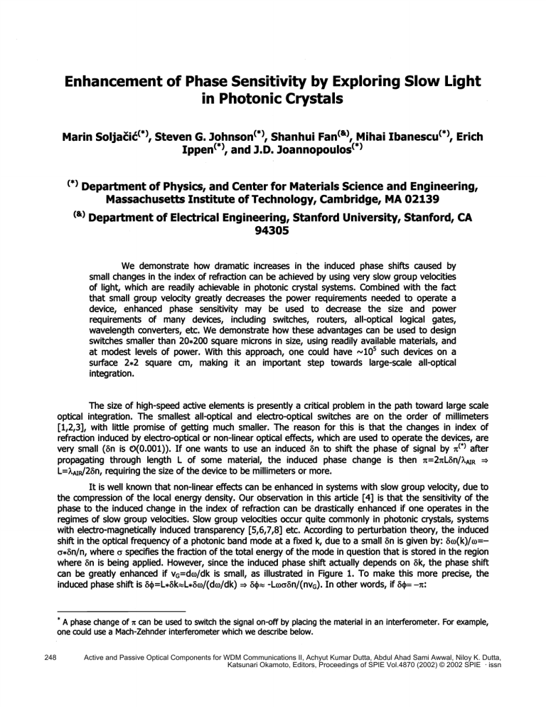
can be greatly enhanced if vG=da/dk is small, as illustrated in Figure 1. To make this more precise, the
induced phase shift is &=L*6kL*&o/(dw/dk) = 64 -LOXJ6n/(nvG). In other words, if &= —it:
* A phase change of it can be used to switch the signal on-off by placing the material in an interferometer. For example,
one could use a Mach-Zehnder interferometer which we describe below.
248
Active and Passive Optical Components for WDM Communications II, Achyut Kumar Dutta, Abdul Ahad Sami Awwal, Niloy K. Dutta,
Katsunari Okamoto, Editors, Proceedings of SPIE Vol.4870 (2002) © 2002 SPIE · issn
AJR
(1)
2a8n)( c)
or for a given n the size of the device scales linearly with vG.
0
9
kAI 2ir
Figure 1: The induced change in the photonic band frequency in a material depends mostly on the
induced index of refraction change. However, depending on the local group velocity, this can lead to
drastically different changes in the wave-vector. Here we show this effect for two dispersion curves: the
slow-light band with v=O.O22c used in a device proposed in this article (thick line), and the dispersion
curve of a uniform material with n=3.5 (thin line). We apply the same frequency shift (&o=O.OO1) to
both of these dispersion curves, to get the respective dashed curves. As we see, the same &o leads to
two very different ak's.
An electro-optical device that is smaller in length by a factor of vs/c also requires vs/c less power to
operate, which is perhaps an even more important consideration for large-scale integration. Thus, for an
electro-optic modulator or a switch, the device enhancement is a factor (v/c)2. The same improvement by
(v/c)2 is achieved in an all-optical gate using the Kerr effect. In this case the on change is self-induced by
the signal itself, and 6n is proportional to the local electric field squared. The savings in the length of the
device is the same vs/c as for an electro-optic device. In addition, because of the small vG, the energy of the
pulse is temporally compressed by a factor of vs/c, so that the induced 6n is 1/(v/c) times larger. Thus, for
a pulse of a fixed total energy, we can actually use a device that is smaller by a factor of "(v/c)2.
IMPROVEMENTS OFFERED BY PHOTONIC CRYSTALS
Photonic crystals (PC's) are ideal systems in which one can achieve arbitrarily low group velocities
[9,10,11]. They are artificially created materials in which the index of refraction has a 1D, 2D, or 3D
periodicity. Under appropriate conditions, and when the maximum index contrast is sufficiently large, a
photonic band-gap appears: a range of frequencies in which light cannot propagate in the crystal. Because
of this, photons inside a PC have many properties similar to electrons in semiconductors. Consequently, PCs
are considered to be a promising media for large-scale integrated optics. In particular, line defects in a PC
can lead to guided mode bands inside the photonic band gap. These bands can in principle be made as flat
as desired by the appropriate design. Typical group velocities for reasonable linear-defect guided modes can
easily be O(102c-103c), thus making it possible to shrink the size of all-optical and electro-optical devices in
PC'S by vG/c)24O4-1O6, while keeping the operating power fixed.
Proc. of SPIE Vol. 4870
249
For definiteness, we focus our attention on a particular class of PC line-defect systems that can have
very low group velocities; namely, we discuss Coupled Cavity Waveguides (CCW) [12,13]. A CCW consists of
many cavities, as in Figure 2. Each of these cavities when isolated supports a resonant mode with the
resonant frequency well inside the band-gap. When we bring such cavities close to each other, to form a
linear defect as in Figure 2, the photons can propagate down the defect by tunneling from one cavity to
another. Consequently, the group velocity is small, and the less closely coupled the cavities are, the slower
the group velocity. Group velocities of c/1000 or even smaller are easy to attain in such systems.
Since the cavities in a CCW are so weakly coupled to each other, the tight-binding method
[12,13,14,15] is an excellent approximation in deriving the dispersion relation. The result is: w(k)=c[1is the single-cavity resonant frequency, A is the physical distance between the
Acx+Kcos(kA)J, where
cavities, and &z<<i<<1 in the tight binding approximation, so we can approximate Aa=O in our analysis.
The CCW system has a zero-dispersion point at k=i/2A. We choose this to be the operation point of
our devices, since the devices in that case have far larger bandwidths than most other slow-light systems
would have; in our simulations, the useful bandwidtWt of such CCW devices is typically more than 1/3 of the
entire CCW band. To see that the CCW system is optimal with respect to bandwidth, we note that in order to
maximize the bandwidth, one wants zkEk(o,n+6n)-k(a,n) to be as independent of co as possible, for as
large a range of a's as possible. One way to satisfy this is, for example, if k(o) is nearly linear, and if the
dominant effect of 6n is to shift k(a) upwards or downwards by a nearly constant amount. This is precisely
what happens in CCW systems. First, note that a(k,6n)=c(1+1)[1+K(1+62)cos(kA)], where 6 and 62 are
first order in n. Thus, n shifts the curve upwards by Q, and also changes the slope at the zero-dispersion
point: K—)K(1+61)(1+2). But, since the slope was so small to start with (since K(<1 in slow-light systems),
the dominant effect in Ak(o,ön) is the linear shift upwards, which produces a term independent of o.
To make the claim from the previous paragraph more precise, we can expand o(k,6n) around the
zero dispersion point, and invert the relation to get k(u,6n), and thereby k(,6n)[61o/c+o2(o/-1)]/AK.
Moreover, since we are working with a slow-light band, we are interested only in co's that can be written as
and since &/<<1, k is almost constant
Thus
(D=c+&o, where
across most of the slow-light band. In fact, a similar derivation can easily be adapted to apply for any zero
dispersion point of any flat dispersion curve. Consequently, if one wants to use slow light to enhance the
non-linear phase sensitivity, one should operate at a zero-dispersion point because this optimizes the
available bandwidth of the device, even in non-CCW systems.
SLOW-LIGHT PHOTONIC CRYSTAL MACH-ZEHNDER DEVICES
To demonstrate how the ideas above can be put to work in practice, we perform numerical
simulation studies of a two-dimensional CCW system. The system is illustrated in Figure 2. It consists of a
square lattice of high-6 dielectric rods (CH=l2.25) embedded in a low-c dielectric material (cL=2.25). The
lattice spacing is denoted by a, and the radius of each rod is r=O.25a. The CCW is created by reducing the
radius of each fourth rod in a line to r/3, so A=4a. We focus our attention on transverse-magnetic (TM)
modes, which have electric field parallel to the rods.
To begin our study of the modes of this system, we perform frequency-domain calculations using
preconditioned conjugate gradient minimization of the Rayleigh quotient in a 2D plane-wave basis as
described in detail in Ref. 16. To model our system, we employ a supercell geometry of size (lla*4a) and a
grid of 72 points per a. The results reveal an 18% photonic band-gap between o)MIN=O.24(2lLc)/a and
(oMAX=O.29(2c)/a. Adding a line defect of CCW's mutually spaced A apart, leads to a CCW band that can be
excellently approximated by a=[O.26522-O.00277cos(kA)](27tc/a). This gives vG=O.0695c at the point of zero
dispersion for the case A=4a. (To demonstrate our ideas, we use a vG that is not extraordinarily small in
For example, in a Mach-Zehnder interferometer, useful bandwidth would be defined as the range of a's in which the
extinction ratio >99% when the device is in its "off" state.
250
Proc. of SPIE Vol. 4870
order to be less demanding on the time-domain numerical simulations.) The frequency-domain calculation
further tells us that roughly 50% of energy of each mode is in the high-c regions, and that this ratio is fairly
independent of k.
,. ... ... ... .
\Ir:i:::'
(C)
\\
•:
.:::.:.:.:.:.:.:...:
(A)
(B)
..:.:. :.
i
:
••.•
•:.
...:.:..:.:.:$..:.:.:........ ...:.:.:.... :
input
..
.
..
..
...... ...t.
:
. :.: . . ..
AcfiveRegon
Figure 2: Sketch of a Mach-Zehnder interferometer that we use to demonstrate enhancement of nonlinear phase sensitivity due to slow-light in photonic crystals. The slow-light system that we use is a
Coupled Cavity Waveguide, as shown in the upper-left inset of this figure. (Throughout the article,
cavities are white to make them more visible). The signal enters the device on the right, is split equally
at the first T-branch into the upper and lower waveguides, and recombined at the T-branch on the left.
If no index change is induced, the parts of the signal coming from the top and the bottom interfere
constructively at the second T-branch, and the pulse exists entirely at the output. If we induce the
index change in the active region in an appropriate manner, the two parts of the signal interfere
destructively, and the pulse is reflected back towards the input, with no signal being observed at the
output. The points marked (A),(B), and (C) correspond to field monitor points during the simulations.
The results of observations from these points are displayed in Figure 3.
To put things in perspective, we can use the frequency-domain code results to estimate sizes of
some real devices. For purposes of illustration only, we simulate a device in which we modify the high-c
material by n/nH=2*1O to perform the switching, say through an electro-optical effect. We pick a
somewhat unrealistically large 6n/nH in order to lower the requirements on our numerical simulations; as
mentioned earlier, the length of the system varies inversely with on/nH and we can scale our results to
experimentally realizable on's accordingly. Let us now ask how long the CCW has to be in order for the signal
to accumulate exactly t phase shift when propagating down this CCW, compared to the case when 6n=O.
We run the frequency domain code twice, using the two different values of CH, for 18 uniformly distributed
k's between k=O, and k at the edge of the first Brillouin zone. Next, we perform the tight-binding curve-fits
to the two sets of data. From these two fitted curves it is trivial to get Ek at the point of zero dispersion, and
thereby L from the relation LAk=ir. The result is that the CCW has to be approximately L=31.6A=35.5?R
long to achieve a r phase shift when propagating down this CCW.
Proc. of SPIE Vol. 4870
251
Switch-ON
Switch-OFF
Obsen'ations at (A)
Observations at (A)
3
3
input pulse
2
LU
A
L
input puise
reflected pu/se
I
1.
Observations at(B)
a5
A
Observations at (C)
Observations at (C)
3
3
output pulse
LU
)0000
TirnE Steps
%/
300000
Time Steps
Figure 3: Demonstration of nonIinear switching in a slow-light photonic crystal system. Electric field
squared as a function of time, observed at three different points: (A),(B), and (C) in the system from
Figure 2. The left column corresponds to the case when no index change is induced; most incoming
signal (A) exits at the output (C). The column on the right corresponds to the case when the non-linear
index change is induced; the signal at the output (C) in the right-hand column is drastically reduced
compared to the output (C) in the left-hand column. The black and dashed-gray signals represent the
pulses traveling from right-to-left, and left-to-right, respectively in Figure 2. The gray pulses are
spurious reflections (mostly from the interface between the photonic crystal and air at the exits of the
device.)
Based on what we learned from the frequency-domain calculations, we can now design a MachZehnder interferometer for use in the time-domain. Specifically, we perform 2D finite-difference time-domain
simulations [17], with perfectly-matched-layer (PML) absorbing boundary conditions [18]. Our numerical
resolution is 24*24 points per a2, meaning that the entire computational cell is 5000*696 points. Since our
computational cell is large enough, we can easily distinguish the pulses reflected from the boundaries of our
simulation, from the real physical pulses. For the waveguides, we use the CCWs as described earlier. The
time-domain simulation reveals that there is a sIowIight band between o)MIN=O.262O(27rc)/a and
coMAX=O.2676(2c)/a, which is within 0.2% of the frequency-domain prediction. Next, we use results of
previous research to implement the needed 90° bends [19], and T branches [20]. At the input of our MachZehnder interferometer, we launch a pulse with a Gaussian frequency profile, with carrier frequency of
o0=O.2648(2irc)/a and FWHM o/ao=1/2OO. During the simulations, we monitor the electric field, E(t), at 8
points in the system. We show the placement of 3 of these points in Figure 2. The observations at the other
5 points (which include the branch points and the end points) provide us with no new information, but are
252
Proc. of SPIE Vol. 4870
monitored just to ensure self-consistency. When on is off, as in the first column of Figure 3, the signal comes
in at the input, splits equally into the two arms at the first branch, and recombines at the second branch,
traveling towards the output, as seen in Figure 4. Apart from very small reflections (app. 2%) due to the
lack of full, optimized branches, most of the signal reaches the output. Next we change the high-index
material to nH—4(l+O.OO166)nH in the upper half of the active region in Figure 2, and nH—(l—O.OO166)nH in
the lower half of the active region in Figure 2(*). Because of this difference in nH, the part of the signal
traveling in the upper arm accumulates it more phase shift than the half traveling in the lower arm. Thus,
the signal interferes destructively at the output, and is reflected back towards the input, as seen in Figure 5.
Even without any fine-tuning, we observe a signal at the output that is 16.4dB smaller than in the case when
n is not applied.
- -) -)
-
;
:-
-
--
-
-
:
:
:
I
--
-
-
--
-
)( - • cØ-)
- C)
3 00)
-
,
-
. - (!-
C''3
G-
))
•-
•
•
-
cC --
-
-
-'
'- . -
.--
-
-
-
:
:-
,.(-tç )
-,
_!•.CC O( :
-o(-: ') C 0
-
.
-
-
:
: :- .
(
(-
-
c-c
-- -
-, -
-
::,
-
- -O- -
(
,
:- _'::::::::: ::_:. ::.:::-:—, :. !'
C C Co -
:
-
-
(!
,', -
-
-
-
-
:
-
-
-
::
'
;? C . C J
--
-
-
-
--
-
.-
-
- - - - - -,
'
.
.
((
:'
Figure 4: Snap-shots of electric field pulse in the system from Figure 2 for the case when no index
change is induced. Top panel is at 120000 time steps, and bottom panel is at 160000 time steps. The
signal entering at the input exits at the output of the device; the device is in its "on" state. (Throughout
the article, cavities are white to make them more visible).
As mentioned before, CCWs have an added benefit in that the bandwidth of the device above is
optimal due to the existence of the zero dispersion point. For example, the useful bandwidth of the device
from Figures 2-5 is &o/cx01/15O. The useful bandwidth of the CCW devices scales roughly linearly with vs/A
for small 6n. On the other hand, the performance gets better with 1/vG2. Therefore, if we are willing to have
a device with a smaller useful bandwidth, we can have a much more efficient device. For example, a
* According to the frequency-domain prediction, the active region therefore needs to be approximately 16 coupled
cavities long if n/nH=O.OO2, we find that we actually need n/nH=O.OOl66 in the time-domain calculation. We attribute
most of the discrepancy to the inadequateness of the tight-binding approximation, finite bandwidth of the beam, and
numerical inaccuracies of the simulations.
§ One might wonder about the practicality of applying a large positive field in one arm and a large negative field in the
other arm of such a tiny device. All that is required, however, is to establish a strong gradient of the field between the
two arms.
Proc. of SPIE Vol. 4870
253
c
0
.Da
9- :2
Q)Q)(J)
L
(I)
G)
cULn
.1-1
0.b
•0
- oj.!?
0 •D
L-
I—
U)
33E
In
a)
I
•D.
)
I-
(0
(C
c0a)
(0
U
°
Q)
'-4 (1)
(n
-:
•5 a)
a)
•D
C
.a) E
0
?0
9
"- C
c: °
t
•D a)
ctu
Q
a)
(I'
4-,
00
:cn
:2>
E1—
(Da)°
2904-'
_o
U)a)
•
.—
4-a (U
0
U)
(Du,
4J
.Ca)
C
> U
0
E
a)
-
u
U)1 U)••D
.2 •q
(Q
'J
<C 4J
.
•D
(0
-'> :a'-I
In a)
.2
.1-I
4-I
.$-I
.-C3 .C
(0
Eu
E
0
5 •j7j Da)
a)
a):"
U
a)
U0. a)CE
- C-
d3
:a
a) (u
•D U)
-0Q •5 E :c -. 0
;O(-
)
(
O.
OO
'DCC
COO
OC'OC
3O
3O
O
00
)OC )C )Q(
C)C C JCOC C OOOCO OOD
DO')C C C )C (OØOO(
3OOC.C OC (OCOCC
O
000c )JO)OOC OC()(
DC
C
OOOO0
00CC
OOC 0 00 ('OC
OOCCC)OO(COOCOC(C(
OuCLCO(
DCCC DC
0O0C0CC 0000
3
00
C
CO
CO
C
,0000u ( OC000C CC
LUOOCOCCO
000 (.OCJ0s0C 0O0OC5 sC COC3C
OO.
0OOO0COCO00OOOC0OC o CO
00 iC0CG0O OOv000 øO')OOC
000C OO0O0OOOOOQOC0GC0C3(
D0DC0O0C00
(0OC0CCOO0 00CC
COOsCO3COO0
)SOCOL 000
CC
SSS
C
OO0
SJs
O
CC
S0COLC'OCS)0OC.
o:
C0SS s3O COO C (000
CO
CCOC3OOOCC COOO C 'D.
O00CC ( 'OC's0Cs ss
C0CCOØ0003C
CL
C5
00CC
S
(
O
0
0 C'(C
( 0O 0
0000'
.jrj cc0,OC0CC
OCOCOC
CsC
0
SCC03S
0L CC0(
0
OCOCOCCO
C
CC
:co
COC000 OO3C SOOC CC OC CC CC
CO
00
0C0C0OOCOCOCO(OsOC
3
S S
525
SCCSCSOO0COC5C5s LO5OCOQ3S3,
C 0000COOC5O'00C0COC COC30000
OC0s0sOOOC0COOOC CCOCCCCSCSS
55 CS0CSCOCOCOOOC0CCSOCO0CDCO
5CO 0300OCL5OO O0OOO0)OCOCOC
O0
OOC000CO
SO
S
0OCOOC0OOCOC0
0OCOOOOOOss0OOOOOOOCCOC 30300
0O00SC303O03O3OO00OS000C003LC
3 00C0s O0O OOUOCC000 00000
S) 3
sOs03000000CCSCCs03000C0000
OC00000C 00C'O€CC SO 0000000
03000 CO 0C00OOOCL
00 CCC COO (CCOCC
00C000OCC
O 00300
(5003000 0 '0300 00C
osCC CC
S
0 0300000 00000000C00CC0C0 S
0 0003 0030C0COCCOOCCO
C OC300
(S
S-S
3OOO)
C0OUCOS0S0O 0300000 SC0OCCCSS
S 3 •3
00O0C0C000sCC
CCC
• OOs00300 0300000COC 00500 0 C C
LSOC00SCS 05S0CL(CCC
5)
0
555
s
5330300 CS0O0OuOC0CCCCOC
sC0Cs00C.
000(505550(5 (OOCCLOOS)
000000 COC0300000000 0 30303
'5) 0C0OCC00u0C000Os0( C0CC00000
555 0300000003030C000C300035 303
30OO00C5,0(OC0C05
C0O00
535)303 (OSS05)0C0O0C C C CCC 0
55
'0
o0000:oooo
•C005S
C . (S
S
55
S
0000 0(00000
0
s
0C
0Co
SSCS50C5S5SC005SS)S
0 0 00 C
Cs
3o
CS0S50(S0C0SOCS(0SS SSS0S 'C's,
5(5 55
S CC COCs
•S)
U00C05'Cs0sC(S(C CC
.5)
05_C C0O0CCC03C00000t (SOC C'30
000OCS3OOO0C0o0CsCOC0s
Co CC
5-SS 0C 0 0C0s0C00
Q
CC
'5
C
55
-S
S5
S
SOSSSC
CC,
300s,C000COCCOQDCCCS
SS SSS5CO00C0
0
00CC
CC
55
0OC
O000C00SO
000oC(
C
030O0
CQ 0
CCO300000 300CCo
( sOC
53355 SO
0 3OSCOC0
0 3uO0
0000o
C
55
C
. C'
so
C
(5
S
5
C
'C
sojss030Css(sstosuos
55-, ,,sCCO00,,ssu'000s0s
OeC,CCC3
''
) s)
oQo o ,
S-- s0OCsC,,sCCCsCCs(0CC0CCs,,
'C
O'
S
'CC'S
" ('00sC"(''
5
C'
s
5'
C,s(
CC CoO
50 35305 'SCs
u,OO0CCO3'3'sos0CCO0C
55-' - n , 3Cs,,Cs(C0COCs
--_0c
' 30(Q0C CCst)D00C, CC
'-S
S
,
0 C'0COC0OC0C0(0(OCC00'
0,0003000O 00(500
S
0
C30C',',Os ',sCOO"Css(S5COCCCCS',s
'C ('CO ("CC CO'OC'OC'
"CC.,
C'
C'CCflC0 (00 0(50500 C 000C3
('C0('
sCC0COoCO(s,sC0C,,o,,so
5,
S
SSOS5C55SSS
SOCS
CS
Os
5555
SC
3500
.
a)
(0
.IJ
.C1E-
a)J
U)
i-4
4J
I- 4J -
0
'I-
_3
a) _C
—
4-a
C
D (0
iz
0
E
E
In
L. D
(0 I
'
0_
C0a)
.C
(0
In
:4J
a)
- a) .2
4-a
—c
E
-'
E
4-a
C
(0 In
C
In
•D
a)
(0a)(0In
C
0_a) II
(1)
0
a).- L_:
:Q
L0 •- •i.JQ) 1
a)
In
a
u> :0 -'
-
j7
>. a)
U)
E
. : •c
In
0
C
4-'
4-
LI-
1
:2
(0
:
_C
't
a) a)
>D
. :O
.C
.
a)
C
a)NInIn
.C
'2 D
4-ac;
0
0. a) .c
00
0.4-'
- - (0 .0a)
.i (0 0._s
—
In In
'
— G)
a) 4-I
(0
a)
UIn
.(
'4—.
0
0
.—
D-4— 0 .C 0 (02f0
0
a)
0.
.D-4
•
In
In
f0
a)
>
b 0'0
a)
.C
4J
U
S0SS
o (0
303530
3
3000
0 SS3 CC0C0O0s00CCOJC
'I- U
XDQ)
3)s0S3Css
0Cf0O3O030C0C
0
0SC0050C00SCC(
0
a)
C
.C
C3OCu0OCCC0O0u0C
Ul—
000030050
000005000005 0(30 D (0 I l)
00 000 (0C00000O 00s0O0C 0 00
rJ
U)s00OCS50s 00CO 0003000000 CC CC
:=
33s
(3353 0 0 0O030C0C0CLCC
C
.4JO4J
35
05(3CC
0 005 00030550000Os. COC
COCS50SSS (CO 05030300000C3000
C0C00S0S SSSSCOCCS 050300000C003o
COS3OS5SS 5C0OS0CSUU00CS0C05 00CC
SC
00 00 03O0
000eO03030000000
C0C
0O 000 C
555
C
3sO C5 SC SC
sss0Oos5C0C
CCs3C 0OOO0Cs 35
0C OQ0CSOS Cs
5CO00O00
CC CC
C C
s53
sO0Q0s
3
000 C05
03
SCCSC
CCC.
:
s30C0C0C0sCsC
0
ssCsC0
SC
C(Css 0CsSC00CSC0C000C0C0s0O0C
0 SC5 (s3Q SO00C(S0000O000000 CC
SOC s3000OCOCs
030300000( 0(00
000000QO0000 000S
00000QOOSCC(SO
00333000003030
0 553 s0s3O0(
0 00030 5000L C 0
0C00OOCO
'00
sC000s300CC00ssss005O0Cs00CC
s03CO0 D30O0C00(s 00C0 30 Cs 0
3O53O5050SOC 55(0S5530C55L55(J
0
00)05505005 S05SS 0C's00s.
5000
0300
000050 C sC3 0C CCss
3
S
($C00QS CC 55
55(555
CCsO 300
C
CO 50 000 55) C 55053000 55 5 55
C
_w s
s(sS0 55 55 C
CC5 sCssssCCs
sQs30
C
S
ss5ss
J0CSSC
053 SOSCSSCSCSOSS
D
C
D
U) a)
CC
.U
'Pa)
U
.
(0
C
(I)
w
U
.!lfl.0 .a
11.
o342
Proc. of SPIE Vol. 4870
254
domain code to calculate (using first order perturbation theory in the small quantity n(r)/n(r)) what
happens to the slow-light band once the non-linear Kerr effect is turned on. We apply the Kerr effect only in
the high index regions, since high index materials typically have non-linear coefficients much higher than
those of low index materials. We now pick physically realistic parameters so that the largest induced ön/n
anywhere is 21O. In this case, the perturbation theory tells us that if we operate at the zero-dispersion
point and the Kerr effect is present in only one arm of the interferometer, the length of the device has to be
7O.97A=175jtm at A=1.55j.tm. The transverse size of the device would then be roughly 2Ojtm. Suppose that
our high-index material has a Kerr coefficient n2=1.5*10'3cm2/W (which is a value achievable in a number of
materials, GaAs at =1.55.tm being one of them), where the Kerr effect is given by n=n2I. In that case,
we would need roughly 0.26W peak power to operate our device. (For comparison, an integrated optics
device made of same (uniform) high index material, with cross section area of O.5j.tm*O.5tm would have to
be 5cm long to operate at the same 0.26W peak power.) The useful bandwidth of our device would be at
least Ao/oo1/67O, meaning that it could operate at bit rates greater than lOOGbit/s. For lower bit rates,
with less bandwidth, the performance enhancements could be even greater. Finally, even the design outlined
here can be further improved by confining more energy into high-c regions, (for example, by using a
triangular-lattice PC system with air holes in dielectric,) or by increasing the index contrast between the
high-c, and low-c materials. By optimizing the design along these lines, one should be able to enhance the
system by additional factors of 3-4 without much effort.
PHOTONIC CRYSTAL 1*2 SWITCH
The switching mechanism in this article is general enough for use in a variety of all-optical logical
operations, switching, routing, wavelength conversion, optical imprinting, etc. For example, we can enhance
the applicability of our design by allowing the device to have two outputs (like in the upper plot of Figure 6),
instead of just one (like in Figure 2). In this case, the non-linear mechanism in question directs input to
either of the two outputs. To achieve this, we put a directional coupler at the output of the device instead of
terminating the device with a simple branch. The directional coupler has to be designed so that (depending
on the relative phase of its two inputs) it directs both of them either to the upper, or the lower of its two
outputs. Almost any directional coupler can be designed to perform this function.
A photonic crystal implementation could be based on the waveguide drop-filter design of Ref. 21.
For this application, we need only to operate it at a frequency offset from that originally intended. An
advantage of this particular design is that it adds only 1X to the length of the entire device. The device of
Ref. 21 involves two linear waveguides and a coupling element (consisting of two point-defect cavities)
between them as shown in the inset of the upper panel of Figure 6. If we label the waveguides as "1" and
"2", we can write:
(
ia
'\
(O—Ot0+za)
co—w0+za)
ia
ia
AQUT1 Ami I
A02
1—
•
I—
(
ia
.
21
I'
=A21— co—co0 +ia JAi[ w—a +ia J,
(2)
where A0uTj, and AINJ are the amplitudes at the output and input of waveguide j, respectively, the central
frequency of the two coupled cavities is o, and 2a is the width of the resonance. In our device, we will have
equal intensities coming to both inputs, and we would like all the energy to exit at a single output. If we look
at this picture from a time-reversed perspective, this tells us that we have to operate the directional coupler
at the frequency coo±a, rather than operating it at co=o, as is done in Ref. 21. This time-reversed picture
also tells us that (according to Eqs.(2)) if we choose to operate at frequency co0+a, we get 100%
transmission at the output of waveguide 2, if the input of waveguide 2 lags waveguide 1 in phase by exactly
ir/2. We get 100% transmission at the output of waveguide 1 if the input of waveguide 2 is ir/2 ahead. The
Proc. of SPIE Vol. 4870
255
dependence of transmission on the phase difference 4 between waveguides 1 and 2 is illustrated in the
lower plot of Figure 6. Operating at the frequency o0—a reverses this relative-phase dependence.
...............
. •IS ••• ••• I
•IIIIIIIIIII•II
IIIIIIIIIIIII•I
11111 •
11111
IllIllIllIllIll
IIIIIIIIIIIIIII
I III III III I
IllIllIllIllIll
:
.A
'I'
t
I
III
......
Output 1
I
:
t
Output 2
Dr
t n ouper
ActfveRegon
+
0
-2
-1.5
-1
-0.5
0
0,5
1
1.5
2
L4 (radians)
Figure 6: Mach-Zehnder interferometer operating as a router between two different outputs. This is
achieved by terminating the interferometer with a directional coupler rather than with a T-branch, as
shown in the upper panel. The lower panel gives the calculated intensity at each of the two outputs, as
a function of the phase difference between the upper and the lower input to the directional coupler.
For example, let's pick as the operating frequency u+a, and let's say that the intensities entering
the device from the two waveguides are the same apart for the fact that waveguide 2 lags waveguide 1 in
phase by ir/2. Then:
'OUTl
(co — (Oo — a)2
—
1+hIN2 2(w_coo)2+a2'
co — co + a)2
IIN1+I1N2 2(co—w0)+a
'OUT2
—
1
(3)
and 1OUT1,OUT2 denote the intensities at the inputs and outputs of the respective waveguides.
According to Eqs.(3), the useful bandwidth of this directional coupler approximately equals 2cc. In contrast to
where 'IN1,1N2
Ref. 21, we are not forced to operate in the regime of very small a; consequently, 2cc can be readily
256
Proc. of SPIE Vol. 4870
designed to be larger than the bandwidth of our Mach-Zehnder interferometer, so the directional coupler will
not impair the performance of the device.
CONCLUDING REMARKS
The sizes of the non-linear devices described in this article using physically realistic values of on are
small enough to have iO of them on a chip of surface size 2cm*2cm, operated at moderate pulse energy
levels, and with speeds greater than lOOGbit/sec. Therefore, we view the work described here as an
important step towards enabling large-scale integration of truly all-optical logic circuits. Finally, it should be
emphasized that all of the results and arguments presented in this paper (which has focused on simplified
2D models) apply immediately to three dimensions. In fact, very recently, new 3D photonic crystal structures
have been introduced that reproduce the properties of linear and point defect modes in 2D photonic crystal
systems [22,23]. Such 3D structures should prove ideal candidates for eventual practical realization of the
non-linear slow-light designs discussed in this work.
This work was supported in part by the Materials Research Science and Engineering Center program
of the National Science Foundation under Grant No. DMR-9400334.
REFERENCES
1.
W.E.Martin: "A new waveguide switch/modulator for integrated optics" AppI. Phys. Lett. 26, 562-564
(1975).
2.
Kawano, K.; Sekine, S.; Takeuchi, H.; Wada, M.; Kohtoku, M.; Yoshimoto, N.; Ito, T.; Yanagibashi,
M.; Kondo, S.; Noguchi, Y.: "4*4 InGaAlAs/lnAlAs MQW directional coupler waveguide switch
modules integrated with spot-size converters and their 10 Gbit/s operation" Electronics Lett. 31, 9697 (1995).
3.
4.
A.Sneh, J.E.Zucker, and B.I.Miller: "Compact, low-crosstalk, and low-propagation-loss quantum-well
Y-branch switches" IEEE Phot. Tech. Lett. 8, 1644-1646 (1996).
Mann Soljai, Steven G. Johnson, Shanhui Fan, Mihai Ibanescu, Erich Ippen, and J.D.
Joannopoulos: "Photonic Crystal Slow-Light Enhancement of Non-linear Phase Sensitivity", an invited
paper in the special issue of JOSA B devoted to Non-linear Photonic Crystals (to appear Sept. 2002).
5.
S.E.Harris: "Electromagnetically Induced Transparency", Physics Today 50, 36-42 (1997).
6.
L.V.Hau, S.E.Harris, Z.Dutton, and C.H.Behroozi: "Light speed reduction to 17 metres per second in
an ultracold atomic gas" Nature 397, 594-598 (1999).
7.
M.O.Scully, M.S.Zubairy, Quantum Optics (Cambridge University Press, Cambridge, 1997).
8.
M.D.Lukin,
9.
E. Yablonovitch: "Inhibited Spontaneous Emission in Solid-State Physics and Electronics", Phys. Rev.
Lett. 58, 2059-2062 (1987).
10.
Sajeev John: "Strong localization of photons in certain disordered dielectric superlattices' Phys. Rev.
Lett. 58, 2486-2489 (1987).
11.
J.DJoannopoulos, R.D.Meade, and J.N.Winn, Photonic Crystals: Mo/ding the flow of light (Princeton
University Press, Princeton, NJ., 1995).
12.
A.Yariv, Y.Xu, R.K.Lee, and A. Scherer: "Coupled-resonator opticalwaveguide:a proposal and
and
A.Imamoglu:
"Controlling
induced transparency" Nature 413, 273-276 (2001).
photons
using
electromagnetically
analysis" Opt. Left. 24, 711-713 (1999).
Proc. of SPIE Vol. 4870
257
13.
M.Bayindir, B.Temelkuran, and E.Ozbay: Tight-Binding Description of the Coupled Defect Modes in
Three-Dimensional Photonic Crystals", Phys. Rev. Left. 84, 2140-2143 (2000).
14.
See, for example, N.W.Ashcroft, and N.D.Mermin, Solid State Physics (Saunders, Philadelphia, PA,
1976).
15.
E. Lidorikis, M. M. Sigalas, E. N. Economou, and C. M. Soukoulis: "Tight-Binding Parametrization for
Photonic Band Gap Materials", Phys. Rev. Left. 81, 1405-1408 (1998).
16.
Steven G. Johnson and 3. D. Joannopoulos: "Block-iterative frequency-domain methods for Maxwell's
equations in a planewave basis" Optics Express 8, no. 3, 173-190 (2001).
17.
For a review, see A.Taflove, Computational Electrodynamics: The Finite-Difference Time-Domain
Method (Artech House, Norwood, Mass., 1995).
18.
J.P.Berenger: "A perfectly matched layer for the absorption of electromagnetic waves", Journal of
Computational Physics, 114, 185-200 (1994).
19.
A.Mekis, J.C.Chen, I.Kurland, S.Fan, P.R.Villeneuve, and J.D.Joannopoulos: "High Transmission
through Sharp Bends in Photonic Crystal Waveguides", Phys. Rev. Left. 77, 3787-3790 (1996).
20.
S.Fan, S.G.Johnson, J.D.Joannopoulos, C.Manolatou, and H.A.Haus: "Waveguide branches in
photonic crystals" J. Opt. Soc. Am. B, 18, 162-165 (2001).
21.
Shanhui Fan, Pierre R.Villeneuve, J.D.Joannopoulos, and H.A. Haus: "Channel Drop Tunneling
through Localized States' Phys. Rev. Lett. 80, 960-963 (1998).
22.
S.G.Johnson, and J.Djoannopoulos: "Three-dimensionally periodic dielectric layered structure with
omnidirectional photonic band gap" AppI. Phys. Lett. 77, 3490-3492 (2000).
23.
M.L.Povinelli, S.G.Johnson, S.Fan, and J.Djoannopoulos: "Emulation of two-dimensional photonic
crystal defect modes in a photonic crystal with a three-dimensional photonic band gap" Phys. Rev. B
64, 075313(1-8) (2001).
258
Proc. of SPIE Vol. 4870
