NEWS & VIEWS LONGWEI YIN AND YOSHIO BANDO*
advertisement
NEWS & VIEWS
SEMICONDUCTOR MORPHOLOGY
Optimizing properties by tuning
morphology
The properties of semiconductors are highly dependent on their structural form.
The finding that ZnS nanobelts can be tuned to take the wurtzite form therefore
adds to the strategies for the control of semiconductor properties by optimization
of size and morphology.
LONGWEI YIN AND YOSHIO BANDO*
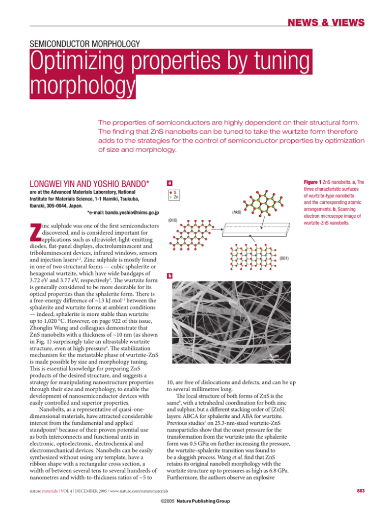
Figure 1 ZnS nanobelts. a, The
three characteristic surfaces
of wurtzite-type nanobelts
and the corresponding atomic
arrangements. b, Scanning
electron microscope image of
wurtzite-ZnS nanobelts.
a
are at the Advanced Materials Laboratory, National
Institute for Materials Science, 1-1 Namiki, Tsukuba,
Ibaraki, 305-0044, Japan.
*e-mail: bando.yoshio@nims.go.jp
S
Zn
(hk0)
(010)
inc sulphide was one of the first semiconductors
discovered, and is considered important for
applications such as ultraviolet-light-emitting
diodes, flat-panel displays, electroluminescent and
triboluminescent devices, infrared windows, sensors
and injection lasers1,2. Zinc sulphide is mostly found
in one of two structural forms — cubic sphalerite or
hexagonal wurtzite, which have wide bandgaps of
3.72 eV and 3.77 eV, respectively3. The wurtzite form
is generally considered to be more desirable for its
optical properties than the sphalerite form. There is
a free-energy difference of ~13 kJ mol–1 between the
sphalerite and wurtzite forms at ambient conditions
— indeed, sphalerite is more stable than wurtzite
up to 1,020 °C. However, on page 922 of this issue,
Zhonglin Wang and colleagues demonstrate that
ZnS nanobelts with a thickness of ~10 nm (as shown
in Fig. 1) surprisingly take an ultrastable wurtzite
structure, even at high pressure4. The stabilization
mechanism for the metastable phase of wurtzite-ZnS
is made possible by size and morphology tuning.
This is essential knowledge for preparing ZnS
products of the desired structure, and suggests a
strategy for manipulating nanostructure properties
through their size and morphology, to enable the
development of nanosemiconductor devices with
easily controlled and superior properties.
Nanobelts, as a representative of quasi-onedimensional materials, have attracted considerable
interest from the fundamental and applied
standpoint5 because of their proven potential use
as both interconnects and functional units in
electronic, optoelectronic, electrochemical and
electromechanical devices. Nanobelts can be easily
synthesized without using any template, have a
ribbon shape with a rectangular cross section, a
width of between several tens to several hundreds of
nanometres and width-to-thickness ratios of ~5 to
Z
(001)
b
3 μm
10, are free of dislocations and defects, and can be up
to several millimetres long.
The local structure of both forms of ZnS is the
same6, with a tetrahedral coordination for both zinc
and sulphur, but a different stacking order of {ZnS}
layers: ABCA for sphalerite and ABA for wurtzite.
Previous studies7 on 25.3-nm-sized wurtzite-ZnS
nanoparticles show that the onset pressure for the
transformation from the wurtzite into the sphalerite
form was 0.5 GPa; on further increasing the pressure,
the wurtzite–sphalerite transition was found to
be a sluggish process. Wang et al. find that ZnS
retains its original nanobelt morphology with the
wurtzite structure up to pressures as high as 6.8 GPa.
Furthermore, the authors observe an explosive
nature materials | VOL 4 | DECEMBER 2005 | www.nature.com/naturematerials
©2005 Nature Publishing Group
883
NEWS & VIEWS
character for the wurtzite-to-sphalerite transformation.
These surprising observations are quite different from
the standard slow transition kinetics observed in the
bulk and ZnS nanoparticles.
It is difficult to understand these intriguing results
from the viewpoint of classical thermodynamics and/
or nanosize-confinement effects. However, surfaceenergy considerations provide a new angle that is
useful to explain this behaviour. Their high surface-tovolume ratio, coupled with the fact that each nanobelt
is a single crystal, make surface effects very prominent
in such materials, and have been shown to greatly
modify equilibrium structure and phase stability
for nanosized materials. Therefore, when reducing
nanocrystal size, surface energy starts to significantly
affect the structural stability.
Wang et al. attribute the exceptional wurtziteZnS structural stability to the particular nanobelt
morphology. The wurtzite-ZnS nanobelt represents
a structure with a lower surface energy than the
sphalerite-ZnS nanoparticles, because the lowestenergy plane in the wurtzite structure corresponds
to the largest surfaces (top and bottom) of the
nanobelts, in direct contrast to the sphalerite
structure. They also find that the nanobelt thickness
plays the key role in their structural stability: below
a critical thickness of 7.4 nm, a wurtzite nanobelt
is found to be more stable than sphalerite. This is
easily understood, because as the nanobelt thickness
is reduced, the surface-to-volume ratio increases,
thereby increasing the relative importance of
surface-energy factors. In addition, structural twins
and faults may provide further stabilization.
The results provide new insights into the
nanobelt-morphology-tuned wurtzite-ZnS
stabilization and wurtzite-to-sphalerite phase
transformation mechanisms within a given nanoscale
object. It also represents an important step towards
harnessing nanoscale semiconductor morphologies
for phase and property optimization8. It indicates that
at ambient conditions, metastable semiconductor
structures with superior properties can be achieved
by careful control of surface, morphology and
size, among which the surface energy is the most
important factor to be considered. This observation
is important for manipulation of the structure
and properties of ZnS nanoscale semiconductors.
Moreover, because most important II–VI and III–V
group wide-bandgap semiconductor materials have
analogous cubic and hexagonal structural forms,
which display different properties suitable for different
applications, the observations by Wang et al. have
implications in the synthesis and designs of other
semiconductor nanomaterials.
The work by Wang and colleagues gives us an idea
of how to optimize phase and properties by selecting
suitable morphology. The proposals raised by the
authors will stimulate new strategies and experiments
with potential technological applications. However,
the puzzle of the morphology control of nanoscale
semiconductors is very complicated. The influence of
the morphology (surface, size, shape, crystallographic
characters) on the phase and properties needs to be
understood in much greater detail.
REFERENCES
1.
2.
3.
4.
5.
6.
7.
8.
Qadri, S. B. et al. Phys. Rev. B 60, 9191–9193 (1999).
Huang, F. & Banfield, J. F. J. Am. Chem. Soc. 127, 4523–4529 (2005).
Kar, S. & Chaudhuri, S. Chem. Phys. Lett. 414, 40–46 (2005).
Wang, Z. W. et al. Nature Mater. 4, 922–927 (2005).
Pan, Z. et al. Science 291, 1947–1949 (2001).
Gilbert, B. et al. Phys. Rev. B 66, 245205 (2002).
Qadri, S. B. et al. J. Appl. Phys. 89, 115–119 (2001).
Chen, C. C. et al. Science 276, 398–401 (1997).
ERRATUM
TURBULENCE AHEAD
b
RUSSELL COWBURN AND DOROTHÉE PETIT
Nature Materials 4, 721–722 (2005).
In this News and Views piece, Figure 1b was
incorrect. It should have appeared as shown here.
Transverse
domain wall
Vortex
domain wall
Figure 1 b, Transverse and vortex domain walls in nanowires.
884
nature materials | VOL 4 | DECEMBER 2005 | www.nature.com/naturematerials
©2005 Nature Publishing Group
