Bio‐Inspired Neuromorphic Systems for Computational Vision
advertisement
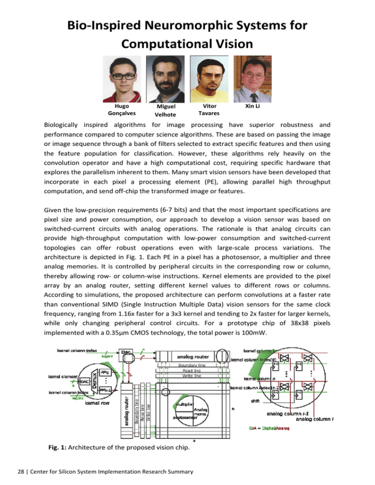
Bio‐Inspired Neuromorphic Systems for Computational Vision Hugo Gonçalves Miguel Velhote Vitor Tavares Xin Li Biologically inspired algorithms for image processing have superior robustness and performance compared to computer science algorithms. These are based on passing the image or image sequence through a bank of filters selected to extract specific features and then using the feature population for classification. However, these algorithms rely heavily on the convolution operator and have a high computational cost, requiring specific hardware that explores the parallelism inherent to them. Many smart vision sensors have been developed that incorporate in each pixel a processing element (PE), allowing parallel high throughput computation, and send off‐chip the transformed image or features. Given the low‐precision requirements (6‐7 bits) and that the most important specifications are pixel size and power consumption, our approach to develop a vision sensor was based on switched‐current circuits with analog operations. The rationale is that analog circuits can provide high‐throughput computation with low‐power consumption and switched‐current topologies can offer robust operations even with large‐scale process variations. The architecture is depicted in Fig. 1. Each PE in a pixel has a photosensor, a multiplier and three analog memories. It is controlled by peripheral circuits in the corresponding row or column, thereby allowing row‐ or column‐wise instructions. Kernel elements are provided to the pixel array by an analog router, setting different kernel values to different rows or columns. According to simulations, the proposed architecture can perform convolutions at a faster rate than conventional SIMD (Single Instruction Multiple Data) vision sensors for the same clock frequency, ranging from 1.16x faster for a 3x3 kernel and tending to 2x faster for larger kernels, while only changing peripheral control circuits. For a prototype chip of 38x38 pixels implemented with a 0.35μm CMOS technology, the total power is 100mW. Fig. 1: Architecture of the proposed vision chip. 28 | Center for Silicon System Implementation Research Summary


