File
advertisement
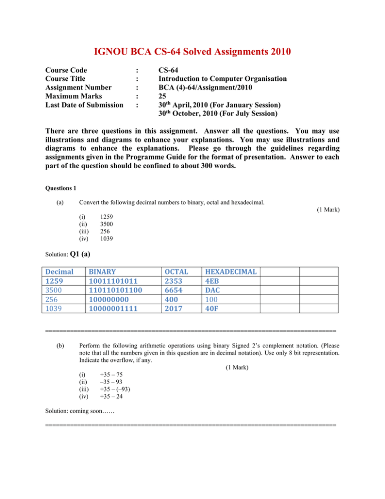
IGNOU BCA CS-64 Solved Assignments 2010 Course Code Course Title Assignment Number Maximum Marks Last Date of Submission : : : : : CS-64 Introduction to Computer Organisation BCA (4)-64/Assignment/2010 25 30th April, 2010 (For January Session) 30th October, 2010 (For July Session) There are three questions in this assignment. Answer all the questions. You may use illustrations and diagrams to enhance your explanations. You may use illustrations and diagrams to enhance the explanations. Please go through the guidelines regarding assignments given in the Programme Guide for the format of presentation. Answer to each part of the question should be confined to about 300 words. Questions 1 (a) Convert the following decimal numbers to binary, octal and hexadecimal. (1 Mark) (i) (ii) (iii) (iv) Solution: Q1 Decimal 1259 3500 256 1039 1259 3500 256 1039 (a) BINARY 10011101011 110110101100 100000000 10000001111 OCTAL 2353 6654 400 2017 HEXADECIMAL 4EB DAC 100 40F ================================================================================== (b) Perform the following arithmetic operations using binary Signed 2’s complement notation. (Please note that all the numbers given in this question are in decimal notation). Use only 8 bit representation. Indicate the overflow, if any. (1 Mark) (i) +35 – 75 (ii) –35 – 93 (iii) +35 – (–93) (iv) +35 – 24 Solution: coming soon…… ================================================================================== (c) Consider an 8-bit data 11100010 along with its Single Error Correcting (SEC) code bits was sent across a communication channel and was received at the destination as 01100010. (You may assume that all the Single Error Correcting code bits that were sent were received correctly at the destination). Find out the SEC bits that were generated at the Source and at the destination of data. Show how these error correcting bits can be used to flag and correct the error in the received data (2 Mark) Solution: coming soon…. ================================================================================== (d) Design and draw a combinational circuit using AND-OR-NOT gates that accepts an input number of three bits. The output of the circuit is a 6 bit number that is the square of the input number. Make the truth table for the circuit and use K-maps to design the circle (1 Mark) Solution: coming soon…. ================================================================================== (e) Draw the circuit for a decoder and explain the working of this decoder. List the possible uses of the decoder circuit. (1 Mark) Decoders can detect a code and activate a single output to signal the presence of that code. Decoders have many applications, from producing system alerts in alarm systems to performing the task of driving multiple devices in microprocessor systems (e.g. memory). Solution: Basic Binary Decoder The function of the binary decoder is to determine if a given input combination has occurred. For example, if we wish to detect that 1011 occurs on the inputs of a digital circuit we must design a decoder which only outputs ‘1’ for this instance. Accordingly, a 4-input AND gate and an Inverter may be employed as illustrated in Figure 2-7. The Three Bit Binary Decoder In order to decode all possible combinations of three bits, eight (23=8) decoding logic gates are required. This type of decoder is called the 3-line-to-8-line decoder because they are 3 inputs and 8 outputs. Let us consider the design of such a decoder and assume that we require ACTIVE HIGH outputs. That is, for a given input combination the decoder outputs ‘1’. To illustrate lets consider Table 2-11 which list the decoding functions and truth tables for the 3-line-to-8-line decoder. Decimal Digit Binary Inputs 0 0 0 1 0 2 Logic Function Outputs D0 D1 D2 D3 D4 D5 D6 D7 0 1 0 0 0 0 0 0 0 0 1 0 1 0 0 0 0 0 0 0 1 0 0 0 1 0 0 0 0 0 3 0 1 1 0 0 0 1 0 0 0 0 4 1 0 0 0 0 0 0 1 0 0 0 5 1 0 1 0 0 0 0 0 1 0 0 6 1 1 0 0 0 0 0 0 0 1 0 7 1 1 1 0 0 0 0 0 0 0 1 Table 2-11 Decoding functions and truth tables for the 3-line-to-8-line decoder Now, we can develop a decoder based on each logic function and implement the SOP logic circuit. This is illustrated below in Figure 2-8. Figure 2-8 Internal Circuitry for 3-line-to-8-line decoder It is far more convenient to use the logic symbol for the3-line-to-8-line decoder as illustrated in Figure 2-9 rather than repeating the complex internal circuitry each time. Figure 2-9 Logic Symbol for 3-line-to-8-line decoder ================================================================================== (f) Explain the concept of Direct mapping Cache memory with the help of an diagram/example. How is this Direct mapping cache different to that of 2 way set associative cache memory? (1 Mark) Solution: Cache Memory - Direct Mapped Cache If each block from main memory has only one place it can appear in the cache, the cache is said to be Direct Mapped. Inorder to determine to which Cache line a main memory block is mapped we can use the formula shown below Cache Line Number = (Main memory Block number) MOD (Number of Cache lines) Let us assume we have a Main Memory of size 4GB (232), with each byte directly addressable by a 32-bit address. We will divide Main memory into blocks of each 32 bytes (25). Thus there are 128M (i.e. 232/25 = 227) blocks in Main memory. We have a Cache memory of 512KB (i.e. 219), divided into blocks of each 32 bytes (25). Thus there are 16K (i.e. 219/25 = 214) blocks also known as Cache slots or Cache lines in cache memory. It is clear from above numbers that there are more Main memory blocks than Cache slots. NOTE: The Main memory is not physically partitioned in the given way, but this is the view of Main memory that the cache sees. NOTE: We are dividing both Main Memory and cache memory into blocks of same size i.e. 32 bytes. A set of 8k (i.e. 227/214 = 213) Main memory blocks are mapped onto a single Cache slot. In order to keep track of which of the 213 possible Main memory blocks are in each Cache slot, a 13-bit tag field is added to each Cache slot which holds an identifier in the range from 0 to 213 – 1. All the tags are stored in a special tag memory where they can be searched in parallel. Whenever a new block is stored in the cache, its tag is stored in the corresponding tag memory location. When a program is first loaded into Main memory, the Cache is cleared, and so while a program is executing, a valid bit is needed to indicate whether or not the slot holds a block that belongs to the program being executed. There is also a dirty bit that keeps track of whether or not a block has been modified while it is in the cache. A slot that is modified must be written back to the main memory before the slot is reused for another block. When a program is initially loaded into memory, the valid bits are all set to 0. The first instruction that is executed in the program will therefore cause a miss, since none of the program is in the cache at this point. The block that causes the miss is located in the main memory and is loaded into the cache. This scheme is called "direct mapping" because each cache slot corresponds to an explicit set of main memory blocks. For a direct mapped cache, each main memory block can be mapped to only one slot, but each slot can receive more than one block. The mapping from main memory blocks to cache slots is performed by partitioning an main memory address into fields for the tag, the slot, and the word as shown below: The 32-bit main memory address is partitioned into a 13-bit tag field, followed by a 14-bit slot field, followed by a 5-bit word field. When a reference is made to a main memory address, the slot field identifies in which of the 214 cache slots the block will be found if it is in the cache. Set Associative mapping scheme combines the simplicity of Direct mapping with the flexibility of Fully Associative mapping. It is more practical than Fully Associative mapping because the associative portion is limited to just a few slots that make up a set. In this mapping mechanism, the cache memory is divided into 'v' sets, each consisting of 'n' cache lines. A block from Main memory is first mapped onto a specific cache set, and then it can be placed anywhere within that set. This type of mapping has very efficient ratio between implementation and efficiency. The set is usually chosen by Cache set number = (Main memory block number) MOD (Number of sets in the cache memory) If there are 'n' cache lines in a set, the cache placement is called n-way set associative i.e. if there are two blocks or cache lines per set, then it is a 2-way set associative cache mapping and four blocks or cache lines per set, then it is a 4-way set associative cache mapping. Let us assume we have a Main Memory of size 4GB (232), with each byte directly addressable by a 32-bit address. We will divide Main memory into blocks of each 32 bytes (25). Thus there are 128M (i.e. 232/25 = 227) blocks in Main memory. We have a Cache memory of 512KB (i.e. 219), divided into blocks of each 32 bytes (25). Thus there are 16K (i.e. 219/25 = 214) blocks also known as Cache slots or Cache lines in cache memory. It is clear from above numbers that there are more Main memory blocks than Cache slots. Cache Size = (Number of Sets) * (Size of each set) * (Cache line size) So even using the above formula we can find out number of sets in the Cache memory i.e. 219 = (Number of Sets) * 2 * 25 Number of Sets = 219 / (2 * 25) = 213. ================================================================================== (g) Differentiate between the access mechanism of a magnetic disk to that of CD ROM? Why do you need a number of disks (RAID)? Define different levels of RAID? (1 Mark) RAID is an acronym first defined by David A. Patterson, Garth A. Gibson, and Randy Katz at the University of California, Berkeley in 1987 to describe a redundant array of inexpensive disks,[1] a technology that allowed computer users to achieve high levels of storage reliability from low-cost and less reliable PC-class disk-drive components, via the technique of arranging the devices into arrays for redundancy. There are various combinations of these approaches giving different trade-offs of protection against data loss, capacity, and speed. RAID levels 0, 1, and 5 are the most commonly found, and cover most requirements. ] RAID 0 RAID 0 (striped disks) distributes data across multiple disks in a way that gives improved speed at any given instant. If one disk fails, however, all of the data on the array will be lost, as there is neither parity nor mirroring. In this regard, RAID 0 is somewhat of a misnomer, in that RAID 0 is non-redundant. A RAID 0 array requires a minimum of two drives. A RAID 0 configuration can be applied to a single drive provided that the RAID controller is hardware and not software (i.e. OS-based arrays) and allows for such configuration. This allows a single drive to be added to a controller already containing another RAID configuration when the user does not wish to add the additional drive to the existing array. In this case, the controller would be set up as RAID only (as opposed to SCSI only (no RAID)), which requires that each individual drive be a part of some sort of RAID array. ] RAID 1 RAID 1 mirrors the contents of the disks, making a form of 1:1 ratio realtime backup. The contents of each disk in the array are identical to that of every other disk in the array. A RAID 1 array requires a minimum of two drives. Although RAID 1's writing process copies the data identically to all drives, a RAID 1 mirror would not be suitable as a permanent backup solution for businesses, since RAID architecture by design allows for certain failures to take place (e.g. vandalism or accidental file deletion). However for home or other applications, where vandalism is very unlikely and accidental file deletion is put up with, RAID 1 offers a good backup solution. RAID 3/4 RAID 3 or 4 (striped disks with dedicated parity) combines three or more disks in a way that protects data against loss of any one disk. Fault tolerance is achieved by adding an extra disk to the array, which is dedicated to storing parity information; the overall capacity of the array is reduced by one disk. A RAID 3 or 4 array requires a minimum of three drives: two to hold striped data, and a third for parity. With the minimum three drives needed for RAID 3, the storage efficiency is 66 percent. With six drives, the storage efficiency is 87 percent. The main disadvantage is poor performance for multiple, simultaneous, and independent read/write operations. RAID 5 Striped set with distributed parity or interleave parity requiring 3 or more disks. Distributed parity requires all drives but one to be present to operate; drive failure requires replacement, but the array is not destroyed by a single drive failure. Upon drive failure, any subsequent reads can be calculated from the distributed parity such that the drive failure is masked from the end user. The array will have data loss in the event of a second drive failure and is vulnerable until the data that was on the failed drive is rebuilt onto a replacement drive. A single drive failure in the set will result in reduced performance of the entire set until the failed drive has been replaced and rebuilt. RAID 6 ================================================================================= (h) What is the need of Direct Memory Access (DMA) in a Single User Computer? What is DMA module? Explain the functions of a DMA module. (1 Mark) Direct memory access is system that can control the memory system without using the CPU. On a specified stimulus, the module will move data from one memory location or region to another memory location or region. While it is limited in its flexibility, there are many situations where automated memory access is much faster than using the CPU to manage the transfers. Systems like the ADC, DAC and PWM capturing all require frequent and regular movements of Solution: memory out of their respective systems. The DMA can be configured to handle moving the collected data out of the peripheral module and into more useful memory locations (like arrays). Only memory can be accessed this way, but most peripheral systems, data registers, and control registers are accessed as if they were memory. The DMA is intended to be used in low power mode because it uses the same memory bus as the CPU and only one or the other can use the memory at the same time. The DMA system is organized into three largely independent parts. Though the three compete for the same memory bus, they have can be configured for independent triggers and memory regions. DMA Operation There are three independent channels for DMA transfers. Each channel receives its trigger for the transfer through a large multiplexer that chooses from among a large number of signals. When these signals activate, the transfer occurs. The DMAxTSELx bits of the DMA Control Register 0 (DMACTL0). The DMA controller receives the trigger signal but will ignore it under certain conditions. This is necessary to reserve the memory bus for reprogramming and nonmaskable interrupts etc. The controller also handles conflicts for simultaneous triggers. The priorities can be adjusted using the DMA Control Register 1 (DMACTL1). When multiple triggers happen simultaneously, they occur in order of module priority. The DMA trigger is then passed to the module whose trigger activated. The DMA channel will copy the data from the starting memory location or block to the destination memory location or block. There are many variations on this, and they are controlled by the DMA Channel x Control Register (DMAxCTL): 1. Single Transfer - each trigger causes a single transfer. The module will disable itself when DMAxSZ number of transfers have occurred (setting it to zero prevents transfer). The DMAxSA and DMAxDA registers set the addresses to be transferred to and from. The DMAxCTL register also allows these addresses to be incremented or decremented by 1 or 2 bytes with each transfer. This transfer halts the CPU. 2. Block Transfer - an entire block is transferred on each trigger. The module disables itself when this block transfer is complete. This transfer halts the CPU, and will transfer each memory location one at a time. This mode disables the module when the transfer is complete. 3. Burst-Block Transfer - this is very similar to Block Transfer mode except that the CPU and the DMA transfer can interleave their operation. This reduces the CPU to 20% while the DMA is going on, but the CPU will not be stopped altogether. The interrupt occurs when the block has completely transferred. This mode disables the module when the transfer is complete. 4. Repeated Single Transfer - the same as Single Transfer mode above except that the module is not disabled when the transfer is complete. 5. Repeated Block Transfer - the same as Block Transfer mode above except that the module is not disabled when the transfer is complete. 6. Repeated Burst-Block Transfer - the same as Burst Block Transfer mode above except that the module is not disabled when the transfer is complete. ================================================================================== (i) What is the concept of Interrupt driven Input/ Output? Assume that while a computer is going through a Read operation from the keyboard, an interrupt occurs that requests for writing a file to the disk. Write the steps that will be involved for the situation as above, if interrupt driven Input/Output is used. Explain each step.(1 Mark) Literally to interrupt means to break the continuity of some on going task. When we talk of computer interrupt we mean exactly the same in terms of the processor. When an interrupt occurs the continuity of the processor is broken and the execution branches to an interrupt service routine. This interrupt service routine is a set of instruction carried out by the CPU to perform or initiate an I/O operation generally. When the routine is over the execution of the CPU returns to the point of interruption and continues with the on going process. Solution: Interrupts can be of two types 1. Hardware interrupts 2. Software interrupts Only difference between them is the method by which they are invoked. Software interrupts are invoked by means of some software instruction or statement and hardware interrupt is invoked by means of some hardware controller generally. InterruptMechanism Interrupts are quite similar to procedures or function because it is also another form temporary execution transfer, but there some differences as well. Note that when procedures are invoked by there names which represents their addresses is specified whereas in case of interrupts their number is specified. This number can be any 8 bit value which certainly is not its address. So the first question is what is the significance of this number? Another thing should also be noticed that procedures are part of the program but the interrupts invoked in the program are no where declared in the program. So the next question is where do these interrupts reside in memory and if they reside in memory then what would be the address of the interrupt? Firstly lets see where do interrupts reside. Interrupts certainly reside somewhere in memory, the interrupts supported by the operating system resides in kernel which you already know is the core part of the operating system. In case of DOS the kernel is io.sys which loads in memory at boot time and in case of windows the kernel is kernel32.dll or kernel.dll. these files contain most of the I/O routines and are loaded as required. The interrupts supported by the ROM BIOS are loaded in ROM part of the main memory which usually starts at the address F000:0000H. Moreover it is possible that some device drivers have been installed these device drivers may provide some I/O routines so when the system boots these I/O routines get memory resident at interrupt service routines. So these are the three possibilities. Secondly a program at compile time does not know the exact address where the interrupt service routine will be residing in memory so the loader cannot assign addresses for interrupt invocations. When a device driver loads in memory it places the address of the services provided by itself in the interrupt vector table. Interrupt Vector Table (IVT) in short is a 1024 bytes sized table which can hold 256 far addresses as each far address occupies 4 bytes. So its possible to store the addresses of 256 interrupts hence there are a maximum of 256 interrupt in a standard PC. The interrupt number is used as an index into the table to get the address of the interrupt service routine. ================================================================================== Questions 2 (a) Write a program to evaluate the following statement: Z = A × B – C ÷ D + A × E using (i) zero address machine instructions (ii) three address machine instructions Explain the difference in the size of the programs. (1 Mark) (b) Assume a machine that has no registers except for PC, AC and MAR. Also assume that the machine has fixed length instructions and have commands for subroutine call and return. For most of the arithmetic instructions in this machine one of the operand is the AC register. Select five addressing modes for the machine. Give reasons for your selection. (1 Mark) (c) Explain the micro-operation sequence that will result in fetching an instruction and executing it. You may assume that it is an ADD instruction which have one direct operand. On execution of this ADD instruction, the direct operand is added to the register AC and the result is left in the AC register. You may assume suitable set of registers for the machine. (1 Marks) Assume that an 8-bit Register R has the binary value 100111001. Perform the following operations on the register R (possibly using another register R2, if needed): (1 Mark) (i) Selective Clear the lower 4 bits of R (ii) Masking out the upper 4 bits of R (iii) Complementing the value of the register R (iv) Inserting a value 0111 in the upper 4 bits of the register R. (d) ================================================================================== (e) Represent 2.0625 and 254.125 into IEEE 754 floating point double precision format. (1 Mark) Solution : 2.0625 = 0f4000800000000000…..254.125 = 0f406FC40000000000 ================================================================================== (f) How a control unit controls the operations of a computer? Explain with the help of an example/diagram. (1 Mark) Control Unit Co-ordinates the input and output devices of a computer system Functions of the Control Unit 1. It controls and monitors the hardware attached to the system to make sure that the commands given to it by the application software are used. For example, if you send something to print, the control unit will keep a check that the instructions are sent to the printer correctly. 2. It controls the input and output of data so that the signals go to the right place at the right time 3. It controls the flow of data within the CPU ================================================================================== (g) What are the micro-instructions? Explain the different types of micros-instructions that can be used in a computer system. Explain the process of micro-instruction execution. (1 Mark) A micro-instruction is a simple command that makes the hardware operate properly. The format is unique to each computer, but our example has a 24 bit micro-instruction. Our instruction is broken down into nine parts: Bits 0-6: ADDR This part of the micro-instruction is used to specify a point in the code to jump to next. Whether or not the jump is made depends upon the result of the ALU operation (see bits 21-23) and the COND field (see bits 7-8). It is just the number of another micro-instruction in the control store. Bits 7&8: COND This part of the micro-instruction determines whether a jump in the code should be made, or if simply the next instruction is to be executed. It can have the following values: o 00: Never jump. o 01: Jump if the ALU's N bit is 1. o 10: Jump if the ALU's Z bit is 1. o 11: Always jump. Bits 9-11: A This part of the micro-instruction is used to determine what register will be the first input to the ALU. It is simply a number from zero to seven. Bits 12-14: B This part of the micro-instruction is used to determine what register will be the second input to the ALU. If the second input is not used, this field's value does not matter. Bits 15-17: C This part of the micro-instruction is used to determine where the output from the ALU is stored, and again is just the number of a register. Bit 18: ENC This part of the micro-instruction is used to determine whether or not the ALU's output is stored in the register specified by the C field (see bits 15-17). If the instruction were just testing to see if a number was zero, for example, the result would not need to be stored anywhere, only the Z flag from the ALU would be important. Bit 19: WR This part of the micro-instruction is used to determine whether or not the contents of the MBR register are written to RAM. It also uses the MAR register to determine which address to write to. Every write takes two cycles (in our example), so a write started in one instruction must be continued in the next. Bit 20: RD This part of the micro-instruction is used to determine if the MBR register is filled with a word from RAM. It uese the MAR register to determine which address to read from. Like a write, a read also requires two cycles. Bits 21-23: ALU This part of the micro-instruction is used to determine what operation the ALU performs on its inputs. o 000: Do nothing, just output the first input o 001: NOT o 010: Left Shift o 011: Right Shift o 100: Add o 101: Subtract o 110: AND o 111: OR An execution unit which is part of a general-purpose microprocessor, partitioned between two integrated circuit chips, with the execution unit on one chip and an instruction unit on another chip. The execution unit provides the interface for accessing a main memory to thereby fetch data and macroinstructions for transfer to the instruction unit when requested to do so by the instruction unit. The execution unit receives arithmetic microinstructions in order to perform various arithmetic operations, and receives access-memory microinstructions in order to develop memory references from logical addresses received from the instruction unit. Arithmetic operations are performed by a data manipulation unit which contains registers and arithmetic capability, controlled by a math sequencer. Memory references are performed by a referencegeneration unit which contains base-and-length registers and an arithmetic capability to generate and check addresses for referencing an off-chip main memory, and is controlled by an access sequencer. TYPES OF MICROINSTRUCTION Each "normal" instruction actually consists of a set of microinstructions. The microinstructions can load an address into the memory address register, cause the value that is referenced by the memory address register into an internal register, or perform some mathematical operation on a value in an internal register. The programmer cannot directly execute microinstruction but can redefine or simply define a set of microinstructions and make an new or improved instruction. This is useful when a piece of software needs to execute some set of operations repeatedly ================================================================================== Questions 3 (a) Q(3) (c) . How is a 16 bit segment address and 16 bit offset of an instruction and data converted to a 20 bit address in 8086 microprocessor? Explain with the help of examples. Give at least two advantages of using such segmentation in 8086 microprocessor. (1 Mark) Q(3) Function 0- Program terminate Action: On execution the call restores vectors for INTS 22h to 24h from the PSP, flushes any buffers and transfers control to the terminate handler address. On entry: AH CS = Segment address of PSP = 0 Returns: Nothing Notes: Equivalent of CP/M BDOS call 00h. INT 21h function 4Ch is preferred. Function 1- Character input with echo Action: Reads a character from the standard input device and echoes it to the standard output device. If no character is ready it waits until one is available. I/O can be re-directed, but prevents detection of OEF. On entry: AH = 01h Returns: AL = 8 bit data input Notes: Equivalent to CP/M BDOS call 01h, except that if the character is CTRL-C an INT 23h is performed. Function 2 - Character output Action: Outputs a character to the standard output device. I/O can be re-directed, but prevents detection of 'disc full'. = On entry: AH DL = 8 bit data (usually ASCII character) 02h Returns: Nothing Notes: Function 3- Auxiliary input Action: Reads a character from the current auxilliary device. On entry: AH = 03h Returns: AL = 8 bit data input Notes: There is no way to read the status of the serial port or to detect errors through this call, therefore most PC comms packages drive the hardware directly, hence their general incompatibility with the 512. Function 4- Auxiliary output Action: Outputs a character to the current auxiliary device. On entry: AH = 04h DL = 8 bit data Returns: Nothing Notes: There is no way to read the status of the serial port or to detect errors through this call. Comments as Function 3. Function 5- Printer output Action: Sends a Character to the current listing device. On entry: AH = 05h DL = 8 bit data Returns: Nothing Notes: If the printer is busy this call will wait until the data is sent. There is no way to poll the printer status in DOS. Function 6- Direct console I/O Action: Reads a character from the standard input device or returns zero if no character available. Also can write a character to the current standard output device. I/O can be redirected but prevents detection of EOF on input or 'disc full' on output. On entry: AH = 06h DL = function requested: 0Ch to 0FEh = output (DL = character to be output) 0FFh = Input request Returns: If output - nothing If input - data ready: zero flag clear, AL = 8 bit data If data not ready: zero flag set Notes: This call ignores CTRL-X. ================================================================================== (b) Explain SAL, DAA, CMP, JMP instructions of 8086 processor with the help of one example each. (1 Mark) SAL memory, REG, immediate immediate memory, REG, CL CL Shift Arithmetic operand1 Left. The number Algorithm: Shift all bits left, the bit that goes off is set to CF. Zero bit is inserted to the right-most position. Example: MOV AL, 0E0h ; AL = 11100000b SAL AL, 1 ; AL = 11000000b, CF=1. RET DAA Decimal adjust After Addition. Corrects the result of addition of two packed BCD values. Algorithm: if low nibble of AL > 9 or AF = 1 then: AL = AL + 6 AF = 1 if AL > 9Fh or CF = 1 then: AL = AL + 60h CF = 1 of shifts is set by operand2. Example: MOV AL, 0Fh ; AL = 0Fh (15) DAA ; AL = 15h RET CMP REG, memory memory, REG REG, REG memory, immediate REG, immediate Compare. Algorithm: operand1 - operand2 result is not stored anywhere, flags are set (OF, SF, ZF, AF, PF, CF) according to result. Example: MOV AL, 5 MOV BL, 5 CMP AL, BL ; AL = 5, ZF = 1 (so equal!) RET JMP label 4-byte address Unconditional Jump. Transfers control to another part of the program. 4-byte address may be entered in this form: 1234h:5678h, first value is a segment second value is an offset. Algorithm: always jump Example: include 'emu8086.inc' ORG 100h MOV AL, 5 JMP label1 ; jump over 2 lines! PRINT 'Not Jumped!' MOV AL, 0 label1: PRINT 'Got Here!' RET ================================================================================= (c) Explain the addressing mode in 8086 microprocessor that can be used for efficient handling of arrays. Explain this with the help of suitable examples. (1 Mark) ================================================================================== (d) Explain any two input and any two output functions of INT 21h for the purpose of input/ output in 8086 microprocessor, with the help of example(s). (1 Mark) ================================================================================== (e) Write a program in 8086 assembly language that compares the first 4 characters of two strings. If the program finds that the compared portion of strings are the same then it also finds the length of the first string. You may assume that both the strings are at least 5 characters long and are available in the data / extra data segment and the last character of the string is #. (2 Marks) ================================================================================== (f) Write a program in 8086 assembly language that multiplies two single digit ASCII numbers. You must first convert these ASCII numbers to equivalent binary. The result of the multiplication must be converted to unpacked decimal number. This resultant unpacked binary coded decimal (BCD) number should have its units digit in AL register and tens digit in AX register. (2 Marks) Multiplication and Division The instructions for multiplication and division are mul and div. Both only operate on the accumulator register (eax) and use the data register (edx) as an overflow. The part of the registers affected are determined by the size of the operand. The following diagram demonstrates how the accumulator and the data registers fit together when being used by the instructions. Therefore, to get expected results, it is recommended that you set edx to zero before calling mul or div. For example: TestProc proc mov eax, 10 xor edx, edx ; set edx to zero mul 10 div 10 ret TestProc endp ==================================================================================
