Op-Amps: Complex Impedance, Differentiators & Integrators
advertisement
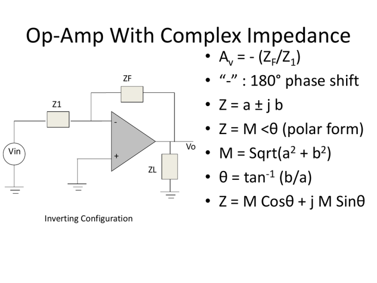
Op-Amp With Complex Impedance ZF Z1 Vin Vo + ZL Inverting Configuration • • • • • • • Av = - (ZF/Z1) “-” : 180° phase shift Z=a±jb Z = M <θ (polar form) M = Sqrt(a2 + b2) θ = tan-1 (b/a) Z = M Cosθ + j M Sinθ Op-Amp With Complex Impedance ZF Z1 Vo + ZL Vin Noninverting Configuration • Av = 1+ (ZF/Z1) • Av = (Z1+ZF)/Z1 Differentiator • Differentiator: circuit whose output is proportional to the derivative of its input • Derivative of a function is the instantaneous slope or rate of change of function • Output of differentiator is proportional to the rate of change of input signal, with respect to time • Output of op amp differentiator will always lag input by 90° (inversion of true derivative) V(t) dv/d t V’(t) Differentiator Operational Amplifiers and Linear Integrated Circuits: Theory and Applications by Denton J. Dailey Differentiator • l Av l = l R/(1/jωC) l = l jωRC l = ωRC • Av = -ωRC <90 = ωRC <-90 R C - Vin Vo + RL Differentiator • Main problem with op amp differentiator is noise sensitivity • Gain of ideal differentiator is zero at dc, and increases with frequency at a rate of 20 dB/decade • High frequency noise will tend to be amplified greatly electronics-tutorials.ws Practical Differentiator RF R1 C - Vin Vo + RL • To reduce gain to high frequency noise, a resistor is placed in series with the input resistor Practical Differentiator • Problem: noise at high frequency • To reduce noise at high frequency a resistor is placed in series with the input capacitor • To reduce noise, R1 < RF • R1 may be chosen such that 10R1< RF to reduce high frequency gain and noise • Before adding R1: Gain characteristics of unmodified differentiator is superimposed on a typical op-amp open-loop Bode plot; differentiator will act correctly up to f0 • After adding R1: differentiator gain levels off at f1 l A l (dB) Practical Differentiator Before adding R1 l A l (dB) AOL AOL f0 Log f f1 = 1/(2πR1C) After adding R1 f1 Log f Differentiation of Nonsinusoidal Inputs • Linear ramp input: V0 = -RCk K: function slope (V/s) • Triangular input: V0 = -RCkn Kn: function slope (V/s) Operational Amplifiers and Linear Integrated Circuits: Theory and Applications by Denton J. Dailey Integrator • Process of integration is complementary to that of differentiation • Relationship is analogous to that between multiplication and division • Function being integrated is called integrand, and dt is called the differential • Integration produces equivalent of the continuous sum of values of function at infinitely many infinitesimally small increments of t • Output of integrator will maintain 90° phase lead, regardless of frequency Integrator V(t) ∫ V(t) dt + C ∫ C1 R1 Vin Vo + RL Operational Amplifiers and Linear Integrated Circuits: Theory and Applications by Denton J. Dailey Integrator • • • • Av = - (ZF/Z1) = - 1/(jωCR) l Av l = l 1/(ωRC) l and phase = 90 Av = 1/(ωRC) <90 f 0 (dc), Av ∞ R1 Vin Reset switch added to force integrator initial conditions to zero Reset C1 Vo + RL Integration of Nonsinusoidal Inputs • • Constant voltage: V0 = -Vin t / RC V0 = 0 at starting Ramp input: V0 = - kt2 / 2R k is rate of change of Vin (V/s) Operational Amplifiers and Linear Integrated Circuits: Theory and Applications by Denton J. Dailey Integrator (Square Wave Input) • V1 = - (Vmt(+))/RC • t(+) = t – t0 • V2 = V1 + [-(Vmt(-))/RC] Operational Amplifiers and Linear Integrated Circuits: Theory and Applications by Denton J. Dailey Integrator • Integrator effectively accumulates voltage over time; presence of input offset voltage will cause capacitor to charge up producing error in output • Smaller the capacitor, more quickly offset error builds up with time • Solutions – – – – – Use of larger capacitor Use of low-offset op amps Bias compensation resistor RB on noninverting terminal Use of resistor RC in parallel with feedback capacitor RC ≥ 10R1 Practical Integrator RC C R1 Vin Vo + RL RB = R1 ll RC
