Low Noise Amplifier Design Amplifier Specification
advertisement
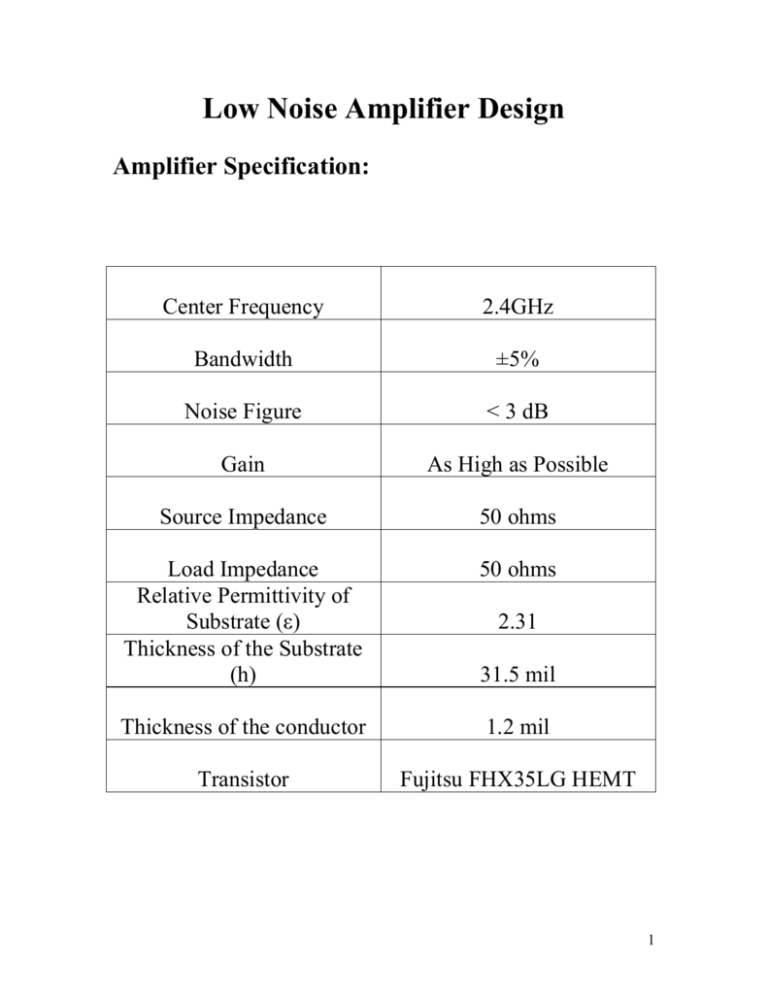
Low Noise Amplifier Design Amplifier Specification: Center Frequency 2.4GHz Bandwidth ±5% Noise Figure < 3 dB Gain As High as Possible Source Impedance 50 ohms Load Impedance Relative Permittivity of Substrate (ε) Thickness of the Substrate (h) 50 ohms Thickness of the conductor 1.2 mil Transistor Fujitsu FHX35LG HEMT 2.31 31.5 mil 1 Design procedure for a given Noise Figure A single stage transistor amplifier with matching networks at the input and output terminals of the transistor are shown below: Zo Gs Go input matching circuit GL output matching circuit transistor [S] Γs Γin Γout Zo ΓL Figure 4.1 a) Check stability performance by calculating Rolette Stability Factor K using the S-parameter of the transistor at the given frequency and plot respective stability circles to determine the potentially unstable region in the Smith Chart for ҐS and ҐL. b) If the transistor is potentially unstable, it can be stabilized by adding a ballast resistor at the drain or a feedback resistor from drain to the source. But this 2 would add to the noise figure. Otherwise we can go for a conditionally stable design. c) Calculate unilateral figure of merit for choosing unilateral or bilateral design. d) Calculate NFmin, Ґopt of the transistor from the SParameter. Then choose a desirable noise figure above the NFmin. Calculate the Centre and radius of the Noise circle. Plot it in the smith chart for Ґin plane. e) For a unilateral case use the constant gain circles for the desired or maximum gain. For a bilateral case use the available power gain circle for the desired or maximum gain. Plot any of these circles accordingly in the Ґin plane. f) Choose a ҐS value which is in the stable region as well as with in the Noise circle, the corresponding circle gain circle. We don’t use operating power gain circles as it has to be plotted in Ґout plane. So it is difficult to correlate with the noise circles in Ґin plane. g) Calculate the corresponding ҐL. From these Ґ values obtain the corresponding impedance values ZS and ZL. 3 h) These are the impedance values for a given noise figure, gain etc for the transistor. Now these have to be matched with their corresponding Source and load impedance Z0 (usually 50 ohms). i) The impedance matching networks (Input and Output) are designed using the smith chart. For e.g. in the input side, the matching network must transform Z0 to ZS. This can be done using lumped elements like LC based network or distributed elements like open or short circuited stubs combined with a length of a transmission line. j) Provide DC bias for the Q point taken from the data sheets and take care that it is transparent with the RF operation. Calculated parameters and design: The S-Parameter file FHX35LG.s2p for the given transistor is downloaded from Fujitsu website. This file is given as an input to a RF utility software called Appcad. Using Appcad the following parameters are calculated at 2.4 GHz as: 4 S11 = 0.925 ∟ -53.0° S21 = 4.200 ∟ 132.5° S12 = 0.050 ∟ 52.5° S22 = 0.500 ∟ -45.0° K = 0.26 < 1 Stability: The transistor is potentially unstable. The stability circles are as given below 5 The unilateral figure of merit is found to be -5.53dB < (Gt/Gtu) < 19.7dB The error range is 25dB which is very high. So we should use bilateral approach. Noise and Gain circles: The Noise parameters at 2.4 GHz are calculated as NFmin = 0.42dB Ґopt = 0.8 ∟38° Rn = 27.4 The desired Noise Figure and the Gain is selected as 1.5 dB and 12 dB 6 The corresponding noise and available gain circles are plotted as given below Figure 4.4 The corresponding ҐS, ҐL, ZS, ZL are found as given below Figure 4.5 7 Impedance Matching networks: The Source impedance matching network should transform 50 ohms to ZS and it is done as given below. The load impedance matching network is as given below The circuit is still not stable at certain frequencies. So a ballast resistor of value 150 ohms was added at the drain. This value was obtained by tuning and optimization in ADS. 8 But this increases the noise figure to 3.128 dB which is not acceptable. Therefore the entire circuit was treated as a 2 port network and the corresponding parameters were calculated once again. The circuit was matched once again at the source and load. The performance in terms of noise figure, gain and stability was very good after the second matching network. Calculations for second matching: S11 = 0.806 ∟ -128.4° S21 = 4.569 ∟ -140° S12 = 0.038 ∟ 146.3° S22 = 0.031 ∟ 66.3° K = 1.085 > 1 NFmin = 1.177dB Ґopt = 0.761 ∟163.86° Rn = 2.017 Then the ҐS, ҐL values are chosen for a noise figure of 2dB and gain 11.5dB 9 The corresponding impedance values are ZS = 5.3 + j6.643 ZL = 33.815 + j6.211 The second matching networks are as given below DC Bias Network: The operating conditions for FHX35LG are read from the data sheet as: 10 Ids = 10 mA Vgs = -0.4V Vds = 3.0V The DC biasing network is designed as given below 11 Amplifier Simulation and Results Schematics and Layout: The Schematics for the amplifier drawn using ADS is shown in the next page. The initial simulations to test the RF performance were done with the S-Parameter file of the transistor. This model doesn’t need biasing circuits. But later the transistor model with a foot print was used, needs inclusion of biasing network. The transmission line dimensions for the Impedance Matching Networks and DC Bias Circuit was calculated using Linecalc – a utility of ADS. After initial Simulations the schematic was transferred in to a layout specific schematic – means some modifications to ensure a proper layout were done. These were 1) Adding Tee networks for branching in the layout. 2) Adding via’s for grounding. 3) Adding a small length of transmission line to connect the pads of devices to other transmission lines. All these modifications were done without affecting the performance. This is shown in figure 5.2 below 12 13 14 The Layout of the amplifier was done using the layout conversion tool of ADS and it is as shown below 15 Simulation and results The circuit was simulated for S-parameter simulation using ADS and various parameters and their performances were noted as given below. S21 and gain at 2.4 GHz Figure 5.4 16 S11 and S22 (return losses): 17 18 Noise Performance: Stability: 19 Measured results: S11 and gain at 2.4 GHz Figure 5.10 The measured gain at 2.4 GHz was 13.986 dB 20 Return loss S11: Figure 5.11 At 2.4 GHz -13.306dB Figure 5.12 21

