High voltage pulser with a fast fall
advertisement
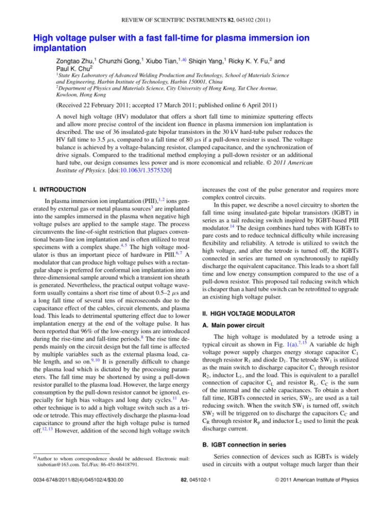
REVIEW OF SCIENTIFIC INSTRUMENTS 82, 045102 (2011) High voltage pulser with a fast fall-time for plasma immersion ion implantation Zongtao Zhu,1 Chunzhi Gong,1 Xiubo Tian,1,a) Shiqin Yang,1 Ricky K. Y. Fu,2 and Paul K. Chu2 1 State Key Laboratory of Advanced Welding Production and Technology, School of Materials Science and Engineering, Harbin Institute of Technology, Harbin 150001, China 2 Department of Physics and Materials Science, City University of Hong Kong, Tat Chee Avenue, Kowloon, Hong Kong (Received 22 February 2011; accepted 17 March 2011; published online 6 April 2011) A novel high voltage (HV) modulator that offers a short fall time to minimize sputtering effects and allow more precise control of the incident ion fluence in plasma immersion ion implantation is described. The use of 36 insulated-gate bipolar transistors in the 30 kV hard-tube pulser reduces the HV fall time to 3.5 μs, compared to a fall time of 80 μs if a pull-down resister is used. The voltage balance is achieved by a voltage-balancing resistor, clamped capacitance, and the synchronization of drive signals. Compared to the traditional method employing a pull-down resister or an additional hard tube, our design consumes less power and is more economical and reliable. © 2011 American Institute of Physics. [doi:10.1063/1.3575320] I. INTRODUCTION In plasma immersion ion implantation (PIII),1, 2 ions generated by external gas or metal plasma sources3 are implanted into the samples immersed in the plasma when negative high voltage pulses are applied to the sample stage. The process circumvents the line-of-sight restriction that plagues conventional beam-line ion implantation and is often utilized to treat specimens with a complex shape.4, 5 The high voltage modulator is thus an important piece of hardware in PIII.6, 7 A modulator that can produce high voltage pulses with a rectangular shape is preferred for conformal ion implantation into a three-dimensional sample around which a transient ion sheath is generated. Nevertheless, the practical output voltage waveform usually contains a short rise time of about 0.5–2 μs and a long fall time of several tens of microseconds due to the capacitance effect of the cables, circuit elements, and plasma load. This leads to detrimental sputtering effect due to lower implantation energy at the end of the voltage pulse. It has been reported that 96% of the low-energy ions are introduced during the rise-time and fall-time periods.8 The rise time depends mainly on the circuit design but the fall time is affected by multiple variables such as the external plasma load, cable length, and so on.9, 10 It is generally difficult to change the plasma load which is dictated by the processing parameters. The fall time may be shortened by using a pull-down resistor parallel to the plasma load. However, the large energy consumption by the pull-down resistor cannot be ignored, especially for high bias voltages and long duty cycles.11 Another technique is to add a high voltage switch such as a triode or tetrode. This may effectively discharge the plasma-load capacitance to ground after the high voltage pulse is turned off.12, 13 However, addition of the second high voltage switch increases the cost of the pulse generator and requires more complex control circuits. In this paper, we describe a novel circuitry to shorten the fall time using insulated-gate bipolar transistors (IGBT) in series as a tail reducing switch inspired by IGBT-based PIII modulator.14 The design combines hard tubes with IGBTs to pare costs and to reduce technical difficulty while increasing flexibility and reliability. A tetrode is utilized to switch the high voltage, and after the tetrode is turned off, the IGBTs connected in series are turned on synchronously to rapidly discharge the equivalent capacitance. This leads to a short fall time and low energy consumption compared to the use of a pull-down resistor. This proposed tail reducing switch which is cheaper than a hard tube switch can be retrofitted to upgrade an existing high voltage pulser. II. HIGH VOLTAGE MODULATOR A. Main power circuit The high voltage is modulated by a tetrode using a typical circuit as shown in Fig. 1(a).7, 15 A variable dc high voltage power supply charges energy storage capacitor C1 through resistor R1 and diode D1 . The tetrode SW1 is utilized as the main switch to discharge capacitor C1 through resistor R2 , inductor L1 , and the load. This is equivalent to a parallel connection of capacitor CL and resistor RL . CC is the sum of the internal and the cable capacitances. To obtain a short fall time, IGBTs connected in series, SW2 , are used as a tail reducing switch. When the switch SW1 is turned off, switch SW2 will be triggered on to discharge the capacitors CC and CR through resistor Rp and inductor L2 used to limit the peak discharge current. B. IGBT connection in series a) Author to whom correspondence should be addressed. Electronic mail: xiubotian@163.com. Tel./Fax: 86-451-86418791. 0034-6748/2011/82(4)/045102/4/$30.00 Series connection of devices such as IGBTs is widely used in circuits with a output voltage much larger than their 82, 045102-1 © 2011 American Institute of Physics 045102-2 Zhu et al. Rev. Sci. Instrum. 82, 045102 (2011) FIG. 2. (Color online) PSPICE simulation of the collector–emitter voltage (VCE ) of IGBTs for different delay time of drive signals and snubber capacitances of 3, 4.7, 7.8, and 10 nF. FIG. 1. Schematic diagram of the HV pulser with the tail reducing switch: (a) main circuit and (b) IGBTs in series. blocking capabilities.16, 17 In our circuit, as shown in Fig. 1(b), the series connection of IGBTs (S1 –Sn ) is only used as a high voltage switch [SW2 in Fig. 1(a)] to release the charge retained in the equivalent capacitance. The biggest difficulty for direct connection of IGBTs in series is unequal voltage sharing across the devices due to the different time delay of the driving circuit or parameter deviations among the different devices.18 The isolated driving signals are delivered by a transformer composed of one primary coil (T0 ) and n secondary coils (T1 –Tn ) to minimize the delay time of the driving circuit. The voltage balancing during the blocking mode (IGBT off state) is achieved using balancing resistors (Rb1 –Rbn ) and snubber capacitors (Cb1 –Cbn ) parallel to the IGBTs. Additionally, a transient voltage suppressor (TVS1 – TVS2 ) is used to protect each IGBT for its fast response to overvoltage. The PSPICE software is utilized to investigate the voltage balance across the IGBTs for different time delay in the drive signal in order to optimize the circuit. Ten kilovolt is used in the simulation and thus ten IGBTs with the ratings of 1200 V are connected. Table I summarizes the parameters of the main components. Figure 2 displays the peak collector–emitter voltages (VCE ) of the IGBTs for different snubber capacitances. When the high voltage (HV) switch SW1 is switched off, the IGBTs connected in series are triggered on. Owing to the asynchronous drive signals, the voltages between the collector and emitter of the IGBTs may increase rapidly and exceed the safety limit of the IGBTs themselves. The parallel snubber capacitors may decrease the rising rate of VCE and clamp it below 1200 V when the time delay is not too long. For example, VCE of the IGBTs for a time delay of 300 ns is only 1080 V with a snubber capacitance of 3 nF. If the time delay becomes longer, big snubber capacitors are needed to further clamp down VCE . However, it may increase the rise time of the HV pulse as well as the energy consumption especially in the high frequency operation modes. Practically, asynchronization of the drive signal should be less than 200 ns to ensure the IGBT group to work reliably. Figure 3 depicts the photograph of the IGBTs connected in series to reduce the voltage tail of high voltage pulses up to 30 kV. The switch consists of 36 IGBTs rated at 1200 V and 25 A. The isolated drive signals of each IGBT are delivered by a transformer with one primary coil and 36 secondary TABLE I. Values of the main components in the simulation circuit. Components Load capacitance Parasitic capacitance Load resistance Snubber capacitances Balancing resistor Current-limited resistor Current-limited resistor Symbol Values Unit CL CC RL Cb1 , Cb2 , . . . , Cb10 Rb1 , Rb2 , . . . , Rb10 Rp L2 4.5 0.5 100 3/4.7/7.8/10 600 100 100 nF nF k nF k μH FIG. 3. (Color online) Photograph of the IGBTs connected in series. 045102-3 Zhu et al. Rev. Sci. Instrum. 82, 045102 (2011) the HV pulse is about 80 μs. In contrast, the IGBTs decrease substantially the fall time, which is only about 3.5 μs if a discharging resistor of 750 is used. More importantly, the snubber capacitances in the tail-biter have very slight influence on the rise time of the HV pulse. III. RESULTS AND DISCUSSION FIG. 4. Drive signal of three IGBTs: (a) during a single pulse; (b) time-axis magnified during the initial process. coils. The precise drive-signal synchronization of each IGBT is crucial to protecting the switch from overvoltage breakdown. The primary coil consists of six parallel coils arrayed along the toroids core to decrease the distance difference along the magnetic circuits, which determine the time delay in each drive signal. Figure 4 shows three drive signals of all the IGBTs detected by the Tektronix TDS1012B-SC oscilloscope and P2220 voltage probe. The pulse width of each drive signal is 25 μs and there is almost no difference in these three signals during the single pulse period as shown in Fig. 4(a). Figure 4(b) shows the drive signals with the time axis magnified as the IGBTs are turned on. The time delay among these three drive signals is about 60 ns and much lower than the value of 200 ns adopted by the simulation above. The other 33 drive signals also exhibit a similar behavior (not displayed here). It is helpful to minimize the energy consumption and detrimental effect on the rise time of the HV pulses from the snubber circuits.19 In our circuits, the snubber capacitance of each IGBT is 7.8 nF, leading to an energy consumption of about 0.0975 J for a single pulse of 30 kV. The energy consumed by the balancing resistors is very small because of the large resistor (600 k). The output voltage on the real resistor load of 24 k is measured by a capacitor divider (1:10 000). Figure 5 displays the pulsed high voltage (30 kV) for different discharging resistor Rp . Without the tail reducing circuit, the fall time of FIG. 5. (Color online) Output pulse voltage on the resistor load of 24 k with different discharging resistor Rp . To demonstrate the performance of the HV modulator consisting of the tail reducing IGBT component, PIII experiments were performed. Figure 6 shows the schematic of the experimental apparatus. The plasma was generated by a direct-current magnetron sputtering system with an Al target 50 mm in diameter. The working gas was argon, flow rate was 11 sccm, and the working pressure was 0.5 Pa. The voltage applied to the magnetron target was about 410 V and the current was 0.41 A. Figure 7(a) displays the waveforms of the HV pulses with various pulse widths with a pull-down resistor of 24 k. On account of to the equivalent capacitance, the fall time of the pulse is up to 80 μs, which is nine times longer than the pulse plateau of 8 μs. This leads to substantial sputtering of the sample. Moreover, much power is wasted by the pull-down resistor. For example, as reported in the literature,20 the average implantation current is 0.2 A for 12 kV pulses. The equivalent impendance of the plasma load calculated by Ohm’s law is 60 k and hence, nearly 71% of the energy of the power supply is consumed by the 24 k pull-down resistor. In contrast, there is no energy consumption in our new system and the fall time of the HV pulse is shortened to 4–5 μs, as is shown in Fig. 7(b). Actually, the fall time can be shrunk even more by increasing the current rate of the IGBTs. Because of the weak dependence of the fall time on the plasma load, the incident ion fluence can be more precisely controlled while sputtering arising from low-energy ions can be significantly reduced. Rapid recovery of the plasma sheath is preferred especially in high-frequency PIII processes. In order to examine the behavior of the plasma sheath, a long probe21 is placed 5 mm from the sample holder. To obtain better signals, a larger probe consisting of a copper stick 6 mm in diameter and 70 mm long is employed. The measurement FIG. 6. Schematic of experimental apparatus. 045102-4 Zhu et al. Rev. Sci. Instrum. 82, 045102 (2011) IV. CONCLUSION FIG. 7. Output waveforms of the HV pulser with different pulse widths on plasma load: (a) with pull-down resistor of 24 k; (b) with tail reducing circuit. voltage Vm applied to the probe is +5 V and the measurement resistor Rm is 100 . The initial current flowing through the probe is about 30–40 mA without turning on the negative high voltage. As soon as the HV pulse (10 kV with pulse width of 20 μs) is applied to the substrate holder, the plasma sheath forms and propagates quickly. The current diminishes rapidly to zero because there are no electrons in the sheath. If the IGBT tail reducing circuit is not used, the plasma sheath does not recover fully until after 200 μs even though the HV pulse (10 μs) has ended much sooner as shown in Fig. 8(a). In contrast, when the IGBTs are used, the plasma sheath collapses rapidly as indicated by the quick increase in the current collected by the probes as demonstrated by Fig. 8(b). A current surge is also observed on the probe and it may be due to a large number of electrons moving from the plasma to the rapidly collapsing sheath. The small recovery time of the plasma sheath enables more conformal PIII processes at high frequencies and/or short pulse widths.22 FIG. 8. (Color online) Recovery characteristics of plasma sheath during a single pulse: (a) without fall time control and (b) with fall time control. A high voltage PIII pulser combining hard tubes and IGBTs is described. A small fall time can be achieved from the HV pulses using 36 IGBTs connected in series to discharge the equivalent capacitance arising from the cable and plasma load. The PSPICE simulation demonstrates that voltage balancing can be accomplished via resistors and snubber circuits in spite of asynchronous 200 ns drive signals. Using 36 IGBTs with relatively low ratings, the long tail of the HV pulse (30 kV) can be effectively clipped. The rise time of the HV pulse is not affected by the IGBT setup whereas the fall time can be reduced to 4–5 μs irrespective of the plasma load and it may be further shortened. The novel modulator enables precise control of the ion fluence, while sputtering can be significantly mitigated. Compared to the traditional use of a pulldown resistor or an additional hard tube, our design is less energy consuming and more economical and reliable. ACKNOWLEDGMENTS This work was financially supported by Natural Science Foundation of China (Nos. 50773015 and 10775036), Program for New Century Excellent Talents in University in China, and Hong Kong Research Grants Council (RGC) Central Allocation Equipment (Grant No. CityU 1/06C). 1 J. R. Conrad, J. I. Radtke, R. A. Dodd, F. J. Worzala, and N. C. Tran, J. Appl. Phys. 62, 4591 (1987). 2 P. K. Chu, S. Qin, C. Chan, N. W. Cheung, and L. A. Larson, Mater. Sci. Eng. R. R17(6–7), 207 (1996). 3 P. K. Chu, B. Y. Tang, L. P. Wang, X. F. Wang, S. Y. Wang, and N. Huang, Rev. Sci. Instrum. 72, 1660 (2001). 4 A. G. Liu, X. F. Wang, B. Y. Tang, and P. K. Chu, J. Appl. Phys. 84, 1859 (1998). 5 X. C. Zeng, T. K. Kwok, A. G. Liu, P. K. Chu, B. Y. Tang, and T. E. Sheridan, IEEE Trans. Plasma Sci. 26, 1 (1998). 6 J. Brutscher, Rev. Sci. Instrum. 67, 2621 (1996). 7 J. O. Rossi, M. Ueda, and J. J. Barroso, Surf. Coat. Technol. 136, 43 (2001). 8 D. T. K. Kwok, M. M. M. Bilek, and D. R. Mckenzie, Appl. Phys. Lett. 82, 1827 (2003). 9 X. B. Tian, L. P. Wang, D. T. K. Kwok, B. Y. Tang, and P. K. Chu, J. Mater. Sci. Technol. 17, 41 (2001). 10 R. A. Stewart and M. A. Lieberman, J. Appl. Phys. 70, 3481 (1991). 11 J. O. Rossi, M. Ueda, and J. J. Barroso, and V. A, Spassov, IEEE Trans. Plasma Sci. 28, 1392 (2000). 12 K. Yukimura and T. Muraho, Nucl. Instrum. Methods Phys. Res. B 206, 791 (2003). 13 K. Yukimura, E. Kuze, and K. Matsunaga, Surf. Coat. Technol. 156, 66 (2002). 14 M. P. J. Gaudreau, J. A. Casey, M. A. Kempkes, T. J. Hawkey, and J. M. Mulvaney, J. Vac. Sci. Technol. B 17, 888 (1999). 15 R. Günzel, A. I. Rogozin, M. Demski, S. N. Rukin, J. Brutscher, and Th. H. G. G. Weise, Surf. Coat. Technol. 156, 54 (2002). 16 J. H. Kim, B. D. Min, S. V. Shenderey, and G. H. Rim, IEEE Trans. Dielectr. Electr. Insul. 14, 921 (2007). 17 P. R. Palmer and A. N. Githiari, IEEE Trans. Power Electron. 12, 637 (1997). 18 K. Sasagawa, Y. Abe, and K. Matsuse, IEEE Trans. Appl. Ind. 40, 1025 (2004). 19 N. Y. A. Shammas, R. Withanage, and D. Chanund, IEE Proc.: Circuits Devices Syst. 153, 34 (2006). 20 C. Z. Gong, X. B. Tian, S. Q. Yang, R. K. Y. Fu, and P. K. Chu, Rev. Sci. Instrum. 79, 043501 (2008). 21 H. C. Wu, G. J. Ma, L. P. Peng, J. J. Feng, H. F. Zhang, and T. C. Ma, Plasma Sci. Technol. 10, 565 (2008). 22 X. B. Tian, X. F. Wang, B. Y. Tang, P. K. Chu, P. K. Ko, and Y. C. Cheng, Rev. Sci. Instrum. 70, 1824 (1999).
