An Ultrawideband CMOS Low-Noise Amplifier for 3.1–10.6
advertisement
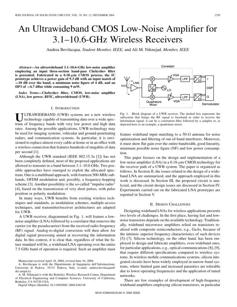
IEEE JOURNAL OF SOLID-STATE CIRCUITS, VOL. 39, NO. 12, DECEMBER 2004 2259 An Ultrawideband CMOS Low-Noise Amplifier for 3.1–10.6-GHz Wireless Receivers Andrea Bevilacqua, Student Member, IEEE, and Ali M. Niknejad, Member, IEEE Abstract—An ultrawideband 3.1–10.6-GHz low-noise amplifier employing an input three-section band-pass Chebyshev filter is presented. Fabricated in a 0.18- m CMOS process, the IC prototype achieves a power gain of 9.3 dB with an input match of 10 dB over the band, a minimum noise figure of 4 dB, and an IIP3 of 6.7 dBm while consuming 9 mW. Index Terms—Chebyshev filter, CMOS, low-noise amplifier (LNA), low power, RFIC, ultrawideband (UWB). I. INTRODUCTION U LTRAWIDEBAND (UWB) systems are a new wireless technology capable of transmitting data over a wide spectrum of frequency bands with very low power and high data rates. Among the possible applications, UWB technology may be used for imaging systems, vehicular and ground-penetrating radars, and communication systems. In particular, it is envisioned to replace almost every cable at home or in an office with a wireless connection that features hundreds of megabits of data per second [1]. Although the UWB standard (IEEE 802.15.3a [2]) has not been completely defined, most of the proposed applications are allowed to transmit in a band between 3.1–10.6 GHz. Two possible approaches have emerged to exploit the allocated spectrum. One is a multiband approach, with fourteen 500-MHz subbands, OFDM modulation and, possibly, a frequency-hopping scheme [3]. Another possibility is the so-called “impulse radio” [4], based on the transmission of very short pulses, with pulse position or polarity modulation. In many ways, UWB benefits from existing wireless techniques and standards, as modulation schemes, multiple-access techniques, and transmitter/receiver architectures are adapted for UWB. A UWB receiver, diagrammed in Fig. 1, will feature a lownoise amplifier (LNA) followed by a correlator that removes the carrier (or the pseudocarrier) from the received radio frequency (RF) signal. Analog-to-digital conversion will then allow for digital signal processing aimed at recovering the information data. In this context, it is clear that, regardless of what the future standard will be, a wideband LNA operating over the entire 7.5-GHz band of operation is required. Such an amplifier must Manuscript received April 18, 2004; revised June 16, 2004. A. Bevilacqua is with the Dipartimento di Ingegneria dell’Informazione, Università di Padova, 35131 Padova, Italy (e-mail: andrea.bevilacqua@ dei.unipd.it). A. M. Niknejad is with the Berkeley Wireless Research Center, Department of Electrical Engineering and Computer Sciences, University of California, Berkeley, CA 94720 USA. Digital Object Identifier 10.1109/JSSC.2004.836338 Fig. 1. Block diagram of a UWB receiver. The dashed box represents the subsystem that brings the RF signal to baseband in order to recover the information signal: it can be a correlation filter followed by a sampler or, as depicted here as an example, a quadrature mixer. feature wideband input matching to a 50- antenna for noise optimization and filtering of out-of-band interferers. Moreover, it must show flat gain over the entire bandwidth, good linearity, minimum possible noise figure (NF) and low power consumption. This paper focuses on the design and implementation of a low-noise amplifier (LNA) in a 0.18- m CMOS technology for the receiver path of a UWB system. The paper is organized as follows. In Section II, the issues related to the design of a wideband LNA are summarized, and the approach employed in this work is discussed. In Section III, the proposed circuit is analyzed, and the circuit design issues are discussed in Section IV. Experiments carried out on the fabricated LNA prototypes are reported in Section V. II. DESIGN CHALLENGES Designing wideband LNAs for wireless applications presents two levels of challenges. In the first place, having fast and lownoise transistors depends on the available technology. Traditionally, wideband microwave amplifiers relied on transistors realized with composite semiconductors, e.g., GaAs, because of the intrinsic superior frequency characteristics of such devices [5]–[7]. Silicon technology, on the other hand, has been employed to design and fabricate amplifiers, even wideband ones, for particular applications, e.g., optical communications [8], [9], that require different specifications compared to wireless systems. In wireless mobile communications systems, silicon integrated circuits have been widely employed in narrow-band systems, where limited gain and increased parasitics are tolerable due to lower operating frequencies and the application of tuned networks. There are few examples of development of high-frequency wideband amplifiers employing silicon transistors, in particular 0018-9200/04$20.00 © 2004 IEEE 2260 IEEE JOURNAL OF SOLID-STATE CIRCUITS, VOL. 39, NO. 12, DECEMBER 2004 Fig. 2. Conceptual schematic of a shunt feedback amplifier. in CMOS technology. In this case, it is remarkable that employed solutions (distributed amplifiers [10]–[12]) require high levels of power consumption, and they are not optimized for noise. This brings about the second challenge—finding a lowpower topology that satisfies all the other design requirements, the most stringent one being the input match. Classic shunt feedback amplifiers have limited input match at higher frequencies due to the parasitic input capacitance. In Fig. 2 a conceptual schematic of a shunt feedback amplifier , is shown. The input impedance is where the gain is chosen such that . As a consequence, the maximum input capacitance that can be tolerated to achieve an input reflection coefficient 10 dB at GHz is as low as equal to fF. Satisfying this requirement with a CMOS amplifier stage while achieving sufficient gain and low noise is difficult. This issue is solved by distributed amplifiers, but at the cost of a power consumption that is five to ten times higher than in a single-stage amplifier, as previously mentioned. Another possibility is balanced amplifiers. In this case, though, the input match is achieved by means of a resistive termination. This results in a degradation of the overall noise performance, as the minimum achievable NF is 3 dB. Moreover, balanced amplifiers require quadrature hybrid couplers that are either narrow band or, if they are wideband, they are multisectional and very large. Thus, they are not amenable to integration. The proposed solution, shown in Fig. 3, expands the use of an inductively degenerated common-source amplifier, a technique widely used in narrow-band designs [13] by embedding the input network of the amplifying device in a multisection reactive network so that the overall input reactance is resonated over a wider bandwidth. A similar technique has enabled narrow-band LNAs to act as multiband concurrent LNAs [14]. In this way, a wideband input match is achieved and, at the same time, good noise performance is attained. In fact, for MOS devices, noise match is very close to power match [13]. To add is placed in series flexibility to the design, an inductor is placed between the gate with the gate, and a capacitor and the source of the input device. The cascode configuration and ) improves the input–output reverse isolation and ( the frequency response of the amplifier. The source-follower is intended for measurement purposes, namely to buffer Fig. 3. Simplified schematic of a wideband LNA. drive an external 50- load. The proposed topology is analyzed in Section III. III. CIRCUIT ANALYSIS The use of inductive local series feedback allows the synthesis of a specified real part for the input impedance equal in a broadband fashion, where is the cutoff freto quency of the transistor. In a narrow-band design, the reactive part of the input impedance is resonated at the carrier frequency. This yields nearly optimal NF at that frequency [13]. In the proposed wideband design, shown in Fig. 3, a doubly terminated three-section passband Chebyshev filter structure is used to resonate the reactive part of the input impedance over the whole band from 3.1 to 10.6 GHz. A. Input Match The input impedance of the MOS transistor with inductive source degeneration is a series RLC circuit (1) . This network is emwhere bedded in the Chebyshev filter structure. A T-network topology is ideally is chosen, as shown in Fig. 4. The real part of chosen to be equal to the source resistance (filter termination), . In the filter passband, the power loss is that is, 0 dB, with a ripple . The choice of reactive elements in the filter determines the bandwidth and the in-band ripple. The input by reflection coefficient is related to (2) The picture described so far is complicated by the presence of the gate–drain capacitance of . The real part of BEVILACQUA AND NIKNEJAD: AN ULTRAWIDEBAND CMOS LNA FOR 3.1–10.6-GHz WIRELESS RECEIVERS Fig. 4. 2261 Schematic of the LNA input network. is decreased with respect to (1). The desired branch series resand the parallel onance is determined by the resonance of and the equivalent capacitance due to the combination of and , i.e., . series combination of also introduces one more parallel resonance and one more series resonance with respect to (1). The parallel resonance essentially . The second series resonance, on the occurs between and and the equivalent capacitance other hand, occurs between and at freresulting from the parallel combination of quencies higher than the parallel resonance. Fig. 5. Impact of parasitic capacitances. The bulk is (a) grounded and (b) connected to the source. B. Gain Analysis To derive the voltage gain of the proposed amplifier, notice , where that the input network impedance is equal to is the Chebyshev filter transfer function. Note that is approximately unity in-band and tends to zero out-of-band. The impedance looking into the amplifier is therefore equal to in-band, and it is very high out-of-band. The current flowing is . At high frequency, the MOS traninto sistor acts as a current amplifier, the current gain being . As a consequence, the output current is, assuming ideal cascode operation, . The load is a shunt-peaking resistor [13]. The overall gain is therefore (3) where is the load resistance, is the load inductance, is the total capacitance between the drain of and and , where is the drain–bulk ground, i.e., capacitance of and is the gate–drain capacitance of . Equation (3) shows that the current gain roll-off is compenintroduces a spurious sated by . Moreover, it shows that resonance with , which must be kept out-of-band. The parasitic capacitances at the source and drain nodes of have a detrimental effect on the amplifier performance. The shunts , as shown in source–bulk capacitance of Fig. 5(a). If the resulting parallel resonance is in-band, the inductive source degeneration is compromised. On the other hand, at lower frequencies, the inductance is boosted. The result is an undesirable frequency dependence in the synthesized real part of the input impedance. The total parasitic capacitance at the drain (sum of , and ) introduces a pole that limits the of bandwidth of the amplifier at high frequencies. The performance of the amplifier is improved by connecting to its source. In this way, is shorted, while the bulk of M Fig. 6. Phase of the drain–source gain for the case of grounded bulk (solid (dash–dotted line). line) and of bulk connected to the source of is connected between the drain and the source of , as illustrated by Fig. 5(b). In order to assess the advantage of this configuration, we compute the voltage gain between the drain and the source nodes. As previously noted, in-band, the input . The current flowing through is current is equal to , and the source voltage is . The voltage at the drain is equal to , where is the total capacitance at the drain node. The drain–source voltage gain is thus (4) Equation (4) shows that the phase of the drain–source gain decreases from 90 at low frequencies to at high frequencies. Both the two high-frequency poles are expected to be out-ofis expected to be around 90 at the band. The phase of lower edge of the band and to decrease to around 0 at the upper edge of the band. As a consequence, due to the Miller effect, the to at higher frequencies is very small. contribution of This results in an enhancement of the bandwidth of the amplifier. This intuitive and very simplified picture is confirmed by is the simulation showed in Fig. 6 where the phase of shown. Note that, at higher frequencies, the presence of other 2262 Fig. 7. IEEE JOURNAL OF SOLID-STATE CIRCUITS, VOL. 39, NO. 12, DECEMBER 2004 Fig. 8. Noise model for the amplifying transistor (b) Input-referred equivalent noise generators. Cross section of a triple-well device. zeros and poles due to circuit elements neglected in the foregoing analysis. In order to connect the bulk terminal to the source terminal, the application of triple-well devices has been explored. However, triple-well devices introduce extra parasitics, as illustrated in Fig. 7. In fact, the bulk terminal tends to be shunted to ground by the parasitic capacitance between the isolated well , as the n-well must be connected to and the n-well to avoid latch-up. We make use of a 1-k isolation resistor. Consequently, the path from the bulk terminal to ground is and the parasitic made up of the series combination of junction capacitance between the n-well and the p-substrate, . Since , this new path is at higher impedance. For the process considered in this design, . The and is thus five times smaller series combination of alone. than in Fig. 3) is needed to drive The source-follower buffer ( an external low-impedance load, i.e., it is required to improve the power gain of the amplifier. The external output voltage is related to the output voltage of the amplifier by (5) where M . (a) M noise sources. way and replaced with two correlated noise generators, as shown in Fig. 8(b): (6) (7) where is the drain noise current, due to the carrier thermal is the induced gate noise, due agitation in the channel, while to the coupling of the fluctuating channel charge into the gate terminal. The induced gate noise and drain current noise power spectral densities are, respectively [13] (8) (9) where 1.33–4, and 0.67–1.33 are excess noise parameis the channel conductance at . ters [15], and The noise voltage can be expressed as the sum of two com, and the other, , uncorreponents, one fully correlated, lated to the noise current as follows: is the external load resistance, i.e., 50 . C. Noise Analysis The noise performance of the proposed topology is determined by two main contributors: the losses of the input network . The noise contribuand the noise of the amplifying device tion of the input network is due to the limited quality factor of the integrated inductors. Its optimization relies on achieving the highest for a given inductance value. The optimization of the relies instead on the choice of its noise contribution from width for a given bias current. Optimum device width has been fully discussed in the literature in the case of narrow-band LNA design [13]. We extend the analysis to the wideband case, i.e., we investigate the amplifier noise behavior over a wide range of frequencies. Optimization is performed on the in-band average NF, as opposed to the spot NF (i.e., NF at a single frequency), used in the narrow-band case. The analysis follows the guidelines of [13] in a dual fashion and with the difference that the loading effect of the local feedback inductor is taken into account. MOS transistor noise sources, shown in Fig. 8(a), are input-referred in a conventional (10) Carrying out the calculations, the correlation impedance written as is (11) where , , and is the correlation coefficient between the gain noise and the drain noise. For MOS is [15]. The parameter devices, the value of accounts for short-channel effects. It describes the transconductance reduction due to velocity saturation and mobility decrease due to vertical fields [13], [16]. BEVILACQUA AND NIKNEJAD: AN ULTRAWIDEBAND CMOS LNA FOR 3.1–10.6-GHz WIRELESS RECEIVERS The two uncorrelated noise sources, by means of the following parameters: and 2263 , are described (12) (13) respectively. By using the introduced parameters, the NF can be expressed by (14) is the source impedance. where Classic noise optimization theory [13], [17] shows that the minimum NF is achieved if the source impedance is chosen such that (15) where, in our case , and (16) Equations (11) and (16) show that the optimum source impedance is roughly the one that resonates the series combiand . As a consequence, nearly minimum NF nation of is achieved over the entire amplifier bandwidth by using the over a wide proposed input network, which produces bandwidth. As a result of the foregoing discussion, the NF of the LNA is (17) where (18) Equations (17) and (18) show that, as , , and, , using a smaller transistor for a given , typically, i.e., drawing more current, is preferable. Moreover, they show that increasing the transconductance improves the noise performance, with all of the other parameters being the same. The LNA NF described by (17) depends on three of the following four quantities: the drain bias current , the over-drive , the transistor width , and the frequency. In order voltage to perform an optimization over the entire band of interest, we consider the average NF. Thus, we reduce the number of independent variables by one. Fig. 9 shows the contour plots of the and . For each value of the average NF as a function of bias current, the device width can be chosen to minimize the Fig. 9. Contour plots of the average NF NF . 5 mA, the best noise performance is NF. In particular, for 450 m. Note that the quantitative reachieved if . The NF sults of Fig. 9 only refer to the noise contribution of in an actual LNA implementation is thus expected to be worse because of: • the losses of the input network, i.e., the limited quality factor of the integrated inductors; noise contribution, particularly • the cascode device significant at higher frequencies; noise contribution; • the load resistance • the output buffer noise contribution. Nonetheless, Fig. 9 gives important insights, as it shows that the noise optimization of the wideband design follows the same guidelines as the narrow-band counterpart. For a given current that yields the best average NF. If budget, there is a value of better noise performance is required, the design can be improved by raising the bias current, as long as the noise performance is . Moreover, note that the NF limited by the contribution of decreases with the scaling of MOS technology. Fig. 10(a) reports the simulated noise contributions due to only (solid line), to the losses of the input network (dashed line), and to the cascode device , the load, and the buffer (dash–dotted line) for the design detailed in Section IV. . In Fig. 10(b), the Note that the main noise contributor is only (solid line), NF is dissected and shown as the noise of by the sum of the noise of and the noise of the three-section input network (dashed line), and by the noise of all the contributors in the circuit (dash–dotted line). Again, the dominant role is clearly illustrated. of IV. CIRCUIT DESIGN The first step in the design is the choice of the input network structure. Given a target input reflection coefficient smaller than 10 dB in-band, (2) yields a ripple 0.46 dB. Values for the normalized components of a filter with such a ripple are found in [18] for several filter prototypes. The components of the actual 2264 IEEE JOURNAL OF SOLID-STATE CIRCUITS, VOL. 39, NO. 12, DECEMBER 2004 M M M M Fig. 10. Noise contributors of the designed LNA. (a) Noise contributions due to (solid line), input network (dashed line), and , load and only (solid line), by and input network (dashed line), and by all circuit components (dash–dotted line). line). (b) NF set by M (dash–dotted TABLE I INPUT NETWORK COMPONENTS filter are obtained by denormalization, setting the appropriate bandwidth (3.1–10.6 GHz) and center frequency (5.7 GHz). Table I shows the component values for a three-section Chebyshev structure and a two-section maximally flat prototype. The three-section structure is chosen as a compromise between filter complexity and component values. Note that the two-section im1.2 pF. This would require an plementation requires that to ensure adequate gain, as shown by (3), extremely high and noise performance, as shown by (17) and (18). The width of (240 m) is optimized for noise. For a given current budget (5 mA), it is sized so that the contributions of thermal and induced gate noise are balanced. The gate–drain makes the input impedance differ from capacitance of a simple series RLC model. The real part is decreased com, as discussed in Section III-A, so that the pared to . The sesource inductance must be set to is approximately determined by and ries resonance of . As a consequence, is set larger . Moreover, must be smaller than , than and boosts the capacitance. as the series combination of Simulation helps in choosing the final values of the components: 1.4 nH, 680 pH, and 100 fF. The cascode device is chosen to be as small as possible to reduce the parasitic capacitances. A lower limit to the width of is set by its noise contribution. The selected value for the is 60 m. Both and are minimum length width of devices (0.18 m). The load is designed to achieve flat gain over the whole bandwidth. The choice of is determined by two opposite must be sizable to have large gain, requirements [see (3)]: out-of-band. and it must be small so that it resonates is chosen to place the zero frequency as close as possible to the lower edge of the band to improve the gain at is set by the voltage lower frequencies. An upper limit to headroom. The values for the components of the load are: 2.6 nH, and . The LNA is biased by means of a current mirror, not shown in is biased through one ac-ground point of Fig. 3 for clarity. the filter. This eliminates the noisy bias isolation resistor. Using 1.8 V, the core power consumption is a power supply 9 mW. The buffer must drive a 50- external load. As a consequence, and the power gain of the LNA is exactly 6 dB lower than the voltage gain of the core amplifier. The buffer is independently biased by means of a current source made up of two transistors in current mirror configuration. The bias current is selected to be 5 mA, and the width of is 60 m. for The transistors used to implement the current source are 100 m wide. They feature a nonminimum length (0.36 m) for higher output impedance. The design has been carried out in two versions: one makes use of standard devices (STD LNA), while the other makes use of triple-well devices (TW LNA). V. MEASUREMENT RESULTS Prototypes have been fabricated in a 0.18- m CMOS process. A microphotograph of the STD LNA is shown in Fig. 11. The layout is very similar in the two versions with the exception of the active devices. Die area including the pads is 1.1 mm . DC pads are electrostatic-discharge (ESD) protected, while RF input and output pads are not. Test measurements have been carried out on wafer. Figs. 12 and 13 show the measured and simulated input and output reflection coefficients, both for the LNA with standard BEVILACQUA AND NIKNEJAD: AN ULTRAWIDEBAND CMOS LNA FOR 3.1–10.6-GHz WIRELESS RECEIVERS Fig. 11. Fig. 14. Measured and simulated power gain for STD and TW LNAs. Fig. 15. Measured and simulated group delay for STD and TW LNAs. 2265 Microphotograph of the LNA employing standard devices. Fig. 12. LNAs. Measured and simulated input reflection coefficient for STD and TW Fig. 13. LNAs. Measured and simulated output reflection coefficient for STD and TW devices (STD LNA) and the one with triple-well devices (TW is lower than 9.9 dB between 2.6–11.7 GHz for the LNA). STD LNA, and lower than 9.4 dB between 2.6–11.5 GHz for the TW LNA. The output buffer achieves excellent matching up to 15 GHz in both cases. In Figs. 14 and 15 the measured and simulated power gain and group delay are reported for both LNAs. The maximum power gain is 9.3 and 10.4 dB for the STD and TW transistors, respectively. Since the output source follower drives a matched load, the voltage gain of the core amplifier is exactly 6 dB higher than . The 3-dB bandwidth is 2.3–9.2 GHz for the STD LNA, while the application of the triple-well brings it to 2.4–9.5 GHz. Group delay decreases from 200 to 130 ps for frequencies increasing from 3 to 4 GHz, while it flattens to 120 ps with a 10-ps ripple in the 4–11-GHz range for both amplifiers. Measured and simulated reverse isolation is depicted in 43 dB, demonstrating Fig. 16. For the STD LNA, the effectiveness of the cascode configuration. In the case of the LNA employing triple-well devices, the connection of the drain–bulk parasitic capacitances between drain and source terminals introduces a feedforward path that brings the 35 dB. input–output isolation to be The -parameters were measured on six different parts for both the STD and the TW LNA. The maximum observed spread of the parameters is less than 1 dB. This result benefits from the use of a ladder-filter input network, a structure well known for its low sensitivity to component variations. It shows, along with the good agreement between measurements and simulation, the robustness of the proposed approach. It is to be noted, though, that, in a production design, packaging parasitics are to be taken 2266 IEEE JOURNAL OF SOLID-STATE CIRCUITS, VOL. 39, NO. 12, DECEMBER 2004 Fig. 19. Circuit model for inclusion of induced gate noise in the simulation. Fig. 16. Measured and simulated reverse isolation for STD and TW LNAs. Fig. 20. Measured two-tone test at 6 GHz for STD and TW LNAs. Inset: Measured IIP3 versus frequency. Fig. 17. Measured quality factor for gate and load inductors. Fig. 21. Fig. 18. Measured two-tone IIP2 for STD and TW LNAs. Measured and simulated spot NF for STD and TW LNAs. into account in the design of the input network. In a bond-wired solution, inductor may be implemented as a bond wire whose inductance is, however, quite unpredictable. Another possibility is to implement the entire - branch externally, so that the pad capacitance is absorbed in , and inductive packaging parasitics add to an external inductor to implement . A preferable solution is to use a bull grid array (BGA) packaging technology. In this case, in fact, the parasitic series inductance is on the order of hundreds of pico-Henry, a quantity comparable to the tolerated component spreads. Two inductors and were included separately as test structures. Their measured quality factor is reported in Fig. 17. In-band, is higher than 8 and 6 for and , respectively. features 10- m-wide traces, versus the 5- m-wide traces of , accounting for the higher . The measured inductance value and and 2.8 self-resonance frequency are 1.5 nH and 23 GHz for nH and 17 GHz for , respectively. Inductor parameter spread over six measured parts is negligible. The measured NF of the two amplifiers is shown in Fig. 18 along with the simulated results. The minimum NF is as low as 4.0 dB (STD) and 4.2 dB (TW), the STD LNA having a slightly BEVILACQUA AND NIKNEJAD: AN ULTRAWIDEBAND CMOS LNA FOR 3.1–10.6-GHz WIRELESS RECEIVERS 2267 TABLE II SUMMARY OF LNA PERFORMANCE, AND COMPARISON WITH PREVIOUSLY PUBLISHED DESIGNS better performance. In a system like the UWB, the average NF is perhaps a better figure of merit than the spot NF. The average NF is 5.2 dB (STD) and 5.3 dB (TW). As discussed in depth in [13], the induced gate noise plays a fundamental role in the optimization of the noise performance of CMOS LNAs. However, the BSIM3 model1 does not include this noise source [19]. We included a subcircuit noise model in our simulations to capture the basic impact of the induced gate noise on the design. The model, shown in Fig. 19, makes use of a resistor as a noise voltage source. The noise voltage is imposed on a capacitor, and the resulting noise current is fed to the output. The spectrum of the output current is therefore proportional to . The main limitation of the subcircuit model is that the generated noise is uncorrelated with the other noise sources present in the circuit, while induced gate noise is partially correlated to the drain current noise. The two-tone test for third-order intermodulation distortion (IIP3) is shown in Fig. 20 for the STD LNA. The test is performed at 6 GHz. Tone spacing is 1 MHz. IIP3 is 6.7 dBm, and the input referred 1-dB compression point (ICP) is 15 dBm. In the inset, Fig. 20 shows IIP3 versus frequency for both LNAs. In the 4–8-GHz range, IIP3 is higher than 8.2 dBm (STD) and 10.8 dBm (TW). Measured second-order intermodulation distortion (IIP2) is reported for both LNAs in Fig. 21 versus frequency. In the 4–8-GHz range, IIP2 is higher than 3 dBm (STD) and 10 dBm (TW). The design does not show particularly high values of IIP2 due to the single-ended topology. The performance shown in Figs. 12–21 allows comparison between the STD and TW LNA designs. The use of triple-well devices accomplishes the goal of pushing the 3-dB cutoff frequency to higher frequencies. However, the achieved bandwidth improvement is smaller than expected from simulation results. 1BSIM4 includes a holistic thermal noise model that does take induced gate noise into account. Moreover, the enhancement of the frequency response of the amplifier comes at the price of a reduction of the reverse isolation and lower linearity. Table II summarizes the performance of the presented amplifiers, with comparison to previously published LNAs. Note that distributed amplifiers generally consume much higher power than the proposed amplifier. VI. CONCLUSION We have demonstrated in this paper a low-power approach for the design of ultrawideband LNAs in the 3.1–10.6-GHz band. The design employs the use of a three-section reactive input network to match an inductively degenerated MOS transistor to a 50- source. This allows us to achieve simultaneously a good antenna termination, low noise, high gain, and high linearity in a wideband fashion, while consuming only 9 mW. The presented design can exploit the CMOS technology evolution trends, both in terms of feature scaling, implying higher speed and lower noise for the active device, and in terms of higher passives. The effectiveness of our approach is supported by experiments carried out on LNA prototypes implemented in a 0.18- m CMOS technology. ACKNOWLEDGMENT The authors would like to thank IBM for IC fabrication and BWRC member companies for their support. The authors also thank A. Berny, C. Doan, and S. Emami for assistance with measurements. REFERENCES [1] S. Stroh, “Ultra-wideband: Multimedia unplugged,” IEEE Spectrum, vol. 40, pp. 23–27, Sept. 2003. [2] (2003) IEEE 802.15 WPAN High Rate Alternative PHY Task Group 3a (TG3a). [Online]. Available: http://www.ieee802.org/ 15/pub/TG3a.html 2268 IEEE JOURNAL OF SOLID-STATE CIRCUITS, VOL. 39, NO. 12, DECEMBER 2004 [3] G. R. Aiello and G. D. Rogerson, “Ultra-wideband wireless systems,” IEEE Microwave Mag., vol. 4, pp. 36–47, Feb. 2003. [4] K. Siwiak, “Ultra-wide band radio: Introducing a new technology,” in Proc. IEEE Vehicular Technology Conf., 2001, pp. 1088–1093. [5] Y. Mimino, M. Hirata, K. Nakamura, K. Sakamoto, Y. Aoki, and S. Kuroda, “High gain-density K-band P-HEMT LNA MMIC for LMDS and satellite communication,” in IEEE Radio Frequency Integrated Circuits Symp. Dig. Papers, 2000, pp. 209–212. [6] Y. Yun, M. Nishijima, M. Katsuno, H. Ishida, K. Minagawa, T. Nobusada, and T. Tanaka, “A fully integrated broad-band amplifier MMIC employing a novel chip-size package,” IEEE Trans. Microwave Theory Tech., vol. 50, pp. 2930–2937, Dec. 2002. [7] P. Marsh, S. Chu, S. Lardizabal, R. Leoni III, S. Kang, R. Wohlert, A. Bowlby, W. Hoke, R. McTaggart, C. Whelan, P. Lemonias, P. McIntosh, and T. Kazior, “Low noise metamorphic HEMT devices and amplifiers on GaAs substrates,” in IEEE Microwave Theory and Techniques Symp. Dig. Papers, 1999, pp. 105–108. [8] Y. Greshishchev, P. Schvan, J. L. Showell, M.-L. Xu, J. J. Ojha, and J. E. Rogers, “A fully integrated SiGe receiver IC for 10-Gb/s data rate,” IEEE J. Solid-State Circuits, vol. 35, pp. 1949–1957, Dec. 2000. [9] J. Cao, M. Green, A. Momtaz, K. Vakilian, D. Chung, K.-C. Jen, M. Caresosa, X. Wang, W.-G. Tan, Y. Cai, I. Fujimori, and A. Hairapetian, “OC-192 transmitter and receiver in standard 0.18- CMOS,” IEEE J. Solid-State Circuits, vol. 37, pp. 1768–1780, Dec. 2002. [10] H.-T. Ahn and D. J. Allstot, “A 0.5–8.5-GHz fully differential CMOS distributed amplifier,” IEEE J. Solid-State Circuits, vol. 37, pp. 985–993, Aug. 2002. [11] R.-C. Liu, K.-L. Deng, and H. Wang, “A 0.6–22-GHz broadband CMOS distributed amplifier,” in IEEE Radio Frequency Integrated Circuits Symp. Dig. Papers, 2003, pp. 103–106. [12] B. M. Ballweber, R. Gupta, and D. J. Allstot, “A fully integrated 0.5–5.5-GHz CMOS distributed amplifier,” IEEE J. Solid-State Circuits, vol. 35, pp. 231–239, Feb. 2000. [13] T. H. Lee, The Design of CMOS Radio-Freqency Integrated Circuits, 1st ed. New York: Cambridge Univ. Press, 1998. [14] H. Hashemi and A. Hajimiri, “Concurrent multiband low-noise amplifiers—Theory, design, and applications,” IEEE Trans. Microwave Theory Tech., vol. 50, pp. 288–301, Jan. 2002. [15] A. J. Scholten, L. F. Tiemeijer, R. van Langevelde, R. J. Havens, A. T. A. Zegers-van Duijnhoven, and V. C. Venezia, “Noise modeling for RF CMOS circuit simulation,” IEEE Trans. Electron Devices, vol. 50, pp. 618–632, Mar. 2003. [16] P. R. Gray, P. J. Hurst, S. H. Lewis, and R. G. Meyer, Analysis and Design of Analog Integrated Circuits, 4th ed. New York: Wiley, 2001. [17] D. M. Pozar, Microwave Engineering. New York: Wiley, 1998. [18] G. Matthaei, L. Young, and E. M. T. Jones, Microwave Filters Impedance-Matching Networks, and Coupling Structures. New York: McGraw-Hill, 1964. m [19] BSIM3v3.2.2 Manual, Univ. of California, Berkeley, 1999. [20] F. Bruccoleri, E. Klumperink, and B. Nauta, “Noise cancelling in wideband CMOS LNAs,” in IEEE ISSCC Dig. Tech. Papers, 2002, pp. 406–407. [21] E. Imbs, I. Telliez, S. Detout, and Y. Imbs, “A low-cost-packaged 4.9–6 GHz LNA for WLAN applications,” in Proc. IEEE Microwave Theory and Techniques Symp., 1999, pp. 1569–1572. Andrea Bevilacqua (S’02) received the Laurea and Ph.D. degrees in electronics engineering from the University of Padova, Padova, Italy, in 2000 and 2004, respectively. From 1999 to 2000, he was an intern with Infineon Technologies, Munich, Germany. From 2002 to 2003, he was a Visiting Scholar with the University of California, Berkeley. His current research interests include the design of RF/microwave integrated circuits and the analysis of wireless communication systems. Ali M. Niknejad (S’93–M’00) received the B.S.E.E. degree from the University of California, Los Angeles, in 1994, and the M.S. and Ph.D. degrees in electrical engineering from the University of California, Berkeley, in 1997 and 2000, respectively. From 2000 to 2002, he was with Silicon Laboratories, Austin, TX, where he was involved with the design and research of CMOS RF integrated circuits and devices for wireless communication applications. Presently, he is an Assistant Professor with the Electrical Engineering and Computer Science Department, University of California, Berkeley. He is an active member at the Berkeley Wireless Research Center (BWRC) and he is the Codirector of the BSIM Research Group. His current research interests lie within the area of analog integrated circuits, particularly as applied to wireless and broadband communication circuits. His interests also include device modeling and numerical techniques in electromagnetics. Dr. Niknejad is currently serving as an Associate Editor of the IEEE JOURNAL OF SOLID-STATE CIRCUITS.
