ECE 3430 – Exam #1
advertisement
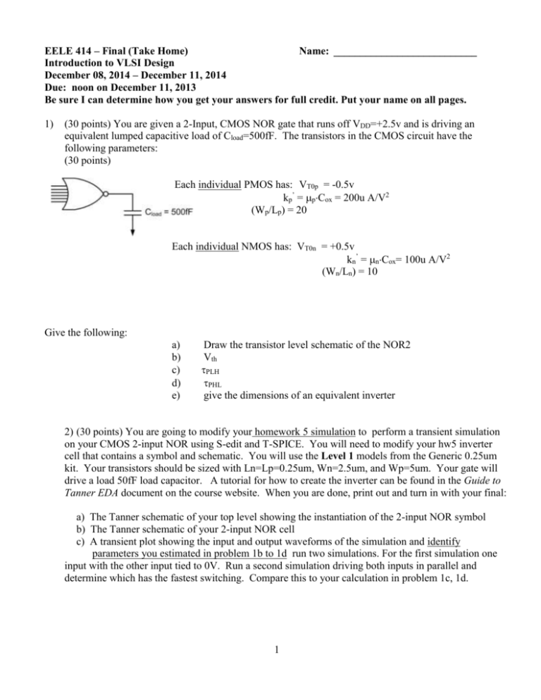
EELE 414 – Final (Take Home) Name: ___________________________ Introduction to VLSI Design December 08, 2014 – December 11, 2014 Due: noon on December 11, 2013 Be sure I can determine how you get your answers for full credit. Put your name on all pages. 1) (30 points) You are given a 2-Input, CMOS NOR gate that runs off VDD=+2.5v and is driving an equivalent lumped capacitive load of Cload=500fF. The transistors in the CMOS circuit have the following parameters: (30 points) Each individual PMOS has: VT0p = -0.5v kp’ = pCox = 200u A/V2 (Wp/Lp) = 20 Each individual NMOS has: VT0n = +0.5v kn’ = nCox= 100u A/V2 (Wn/Ln) = 10 Give the following: a) b) c) d) e) Draw the transistor level schematic of the NOR2 Vth PLH PHL give the dimensions of an equivalent inverter 2) (30 points) You are going to modify your homework 5 simulation to perform a transient simulation on your CMOS 2-input NOR using S-edit and T-SPICE. You will need to modify your hw5 inverter cell that contains a symbol and schematic. You will use the Level 1 models from the Generic 0.25um kit. Your transistors should be sized with Ln=Lp=0.25um, Wn=2.5um, and Wp=5um. Your gate will drive a load 50fF load capacitor. A tutorial for how to create the inverter can be found in the Guide to Tanner EDA document on the course website. When you are done, print out and turn in with your final: a) The Tanner schematic of your top level showing the instantiation of the 2-input NOR symbol b) The Tanner schematic of your 2-input NOR cell c) A transient plot showing the input and output waveforms of the simulation and identify parameters you estimated in problem 1b to 1d run two simulations. For the first simulation one input with the other input tied to 0V. Run a second simulation driving both inputs in parallel and determine which has the fastest switching. Compare this to your calculation in problem 1c, 1d. 1 3) (10 points) For the following CMOS circuit, give the dimensions of an equivalent inverter: 2 4) (10 points) For the following Transmission Gate, give the equivalent ON resistance: VT0n = |VT0p| = 1v kn = nCox(Wn/Ln) = 300u A/V2 kp = pCox(Wp/Lp) = 150u A/V2 5) (15 points) If you could design a perfect CMOS inverter with VDD=+2.5v, what would the following values be? a) VOH = b) VOL = c) VIH = d) VIL = e) VTH = f) NMH = g) NML = 6) (5 points) If you are analyzing an NMOS transistor and notice that it is ON and that Vg=Vd are at the same potential, what region of operation is it in? 3
