2012
advertisement
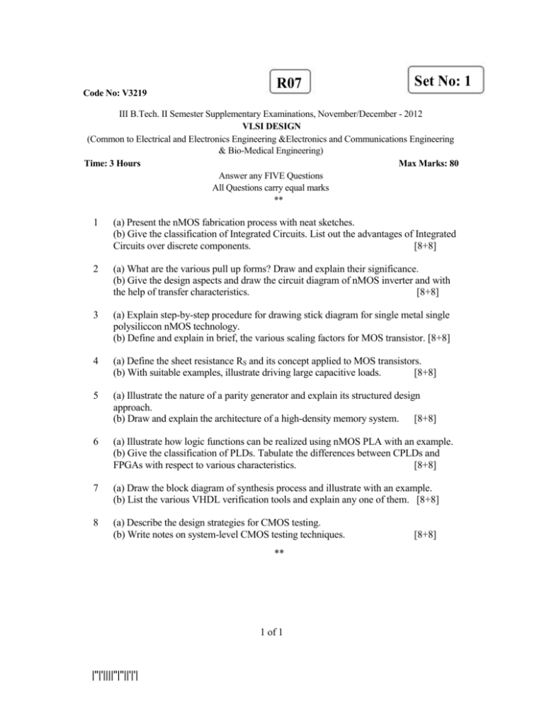
Code No: V3219 R07 Set No: 1 III B.Tech. II Semester Supplementary Examinations, November/December - 2012 VLSI DESIGN (Common to Electrical and Electronics Engineering &Electronics and Communications Engineering & Bio-Medical Engineering) Time: 3 Hours Max Marks: 80 Answer any FIVE Questions All Questions carry equal marks ** 1 (a) Present the nMOS fabrication process with neat sketches. (b) Give the classification of Integrated Circuits. List out the advantages of Integrated Circuits over discrete components. [8+8] 2 (a) What are the various pull up forms? Draw and explain their significance. (b) Give the design aspects and draw the circuit diagram of nMOS inverter and with the help of transfer characteristics. [8+8] 3 (a) Explain step-by-step procedure for drawing stick diagram for single metal single polysiliccon nMOS technology. (b) Define and explain in brief, the various scaling factors for MOS transistor. [8+8] 4 (a) Define the sheet resistance RS and its concept applied to MOS transistors. (b) With suitable examples, illustrate driving large capacitive loads. [8+8] 5 (a) Illustrate the nature of a parity generator and explain its structured design approach. (b) Draw and explain the architecture of a high-density memory system. [8+8] 6 (a) Illustrate how logic functions can be realized using nMOS PLA with an example. (b) Give the classification of PLDs. Tabulate the differences between CPLDs and FPGAs with respect to various characteristics. [8+8] 7 (a) Draw the block diagram of synthesis process and illustrate with an example. (b) List the various VHDL verification tools and explain any one of them. [8+8] 8 (a) Describe the design strategies for CMOS testing. (b) Write notes on system-level CMOS testing techniques. ** 1 of 1 |''|'||||''|''||'|'| [8+8] Code No: V3219 R07 Set No: 2 III B.Tech. II Semester Supplementary Examinations, November/December - 2012 VLSI DESIGN (Common to Electrical and Electronics Engineering &Electronics and Communications Engineering & Bio-Medical Engineering) Time: 3 Hours Max Marks: 80 Answer any FIVE Questions All Questions carry equal marks ** 1 (a) Classify different types of major processes used in IC fabrication and also give the classification of integrated circuits. (b) Explain the concepts of ‘Lithography’ and ‘Probe testing’ related to IC production process. [8+8] 2 (a) Deduce the expressions for drain-to-source current versus drain-to- source voltage relations. (b)Draw the circuit diagram of CMOS inverter and give its design considerations. [8+8] (a)Explain with suitable diagrams, the lambda-based design rules. (b) Draw the symbolic layout for the CMOS inverter and give the general CMOS logic-gate layout guidelines. [8+8] 3 4 (a) What is meant by Switch Logic? Explain some switch logic arrangements. (b) Explain in detail about formal estimation of CMOS Inverter delay. [8+8] 5 (a) Give the subsystem design considerations of a four-bit adder. (b) Explain Two’s Complement multiplication using the Baugh-Wooley method. [8+8] 6 (a) Differentiate PAL and PLA with respect to various performance parameters. (b) Compare the performance parameters of Complex Programmable Logic Devices and Field Programmable Gate Arrays. [8+8] 7 (a) Describe the following relevant to VHDL synthesis. (i)Simulation (ii) layout (b) With suitable block diagrams, explain the terms ‘Hardware Simulation’ and ‘Synthesis Process’. [8+8] 8 (a) What is meant by CMOS testing? Explains its design strategies. (b) What are the system-level test techniques? Explain one of them with suitable example. [8+8] ** 1 of 1 |''|'||||''|''||'|'| Code No: V3219 R07 Set No: 3 III B.Tech. II Semester Supplementary Examinations, November/December - 2012 VLSI DESIGN (Common to Electrical and Electronics Engineering &Electronics and Communications Engineering & Bio-Medical Engineering) Time: 3 Hours Max Marks: 80 Answer any FIVE Questions All Questions carry equal marks ** 1 2 (a) Tabulate the comparison of various MOS Technologies available with respect to important characteristics. (b) Explain step-by-step procedure for a typical n-well process with neat diagrams. [8+8] (a) Draw and explain the characteristics of nMOS transistor in different modes of operation and its body effect. (b) Discuss on MOS transistor threshold voltage. [8+8] 3 (a) Draw and explain in detail about ‘VLSI Design Flow’. (b) Define any four scaling factors for MOS device parameters and give their expressions. [8+8] 4 (a) What is meant by sheet resistance RS? Explain the concept of Rs applied to MOS transistors. (b) Explain the concepts of ‘nMOS inverter pair delay’ and ‘Minimum size CMOS inverter pair delay ‘with necessary circuit diagrams. [8+8] 5 (a) What are Wallace tree elements? Give and explain an example of the Wallace tree approach. (b) Explain step-by-step design approach for subsystem design using adder as an example. [8+8] 6 (a) Draw the general architecture of programmable logic array and explain. (b) Differentiate Complex Programmable Logic Devices and Field Programmable Gate Arrays with respect to various performance parameters and their architectural views. [8+8] 7 7(a) Explain any one of the design capture tools available for VHDL synthesis with an example. (b) Explain the VHDL Synthesis process with the help of neat schematic diagram. [8+8] (a) Explain the CMOS testing principles. (b) Discuss about chip level test techniques relevant to CMOS testing. [8+8] ** 8 1 of 1 |''|'||||''|''||'|'| Code No: V3219 R07 Set No: 4 III B.Tech. II Semester Supplementary Examinations, November/December - 2012 VLSI DESIGN (Common to Electrical and Electronics Engineering &Electronics and Communications Engineering & Bio-Medical Engineering) Time: 3 Hours Max Marks: 80 Answer any FIVE Questions All Questions carry equal marks ** 1 (a) Explain the IC production process concept of ‘Oxidation’ and ‘Ion Implantation’. (b) Tabulate the comparison between CMOS and Bipolar technologies. [8+8] 2 (a) Determine the pull-up to pull-down ratio for an nMOS inverter driven by another nMOS inverter. (b) Explain the design considerations of Bi-CMOS inverter with suitable circuit diagram. [8+8] 3 (a) What are limitations of scaling for VLSI circuits and briefly explain them. (b) Tabulate the encoding scheme for a simple single metal nMOS process with respect to various MOS layers. [8+8] 4 (a) Discuss about area capacitances of MOS layers and give area capacitance calculations with suitable examples. (b)What are the alternate gate circuits are available? Explain any one of item with suitable sketch. [8+8] 5 (a) Elaborate the concept of pipelining relevant to subsystem design principles. (b) Draw a four-bit Braun multiplier and give its subsystem level design considerations. [8+8] 6 (a) Illustrate with an example how logic functions can be realized using nMOS PLA. (b) Explain the design flow of standard cell with neat diagram. [8+8] (a) Explain the advantages, applications and types of Simulation relevant to VLSI Design flow. (b) Explain the following with respect to VHDL synthesis. (i)Simulation (ii) layout [8+8] 7 8 (a) Explain the concept of layout design for improved testability with suitable example. (b)Write notes on system-level CMOS testing techniques. [8+8] ** 1of 1 |''|'||||''|''||'|'|
