Supplemental Information_Part2_FINAL_DRAFT
advertisement
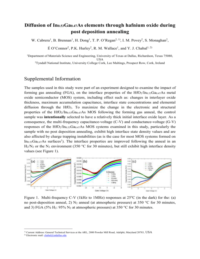
Diffusion of In0.53Ga0.47As elements through hafnium oxide during post deposition annealing W. Cabrera1, B. Brennan1, H. Dong1, T. P. O’Regan2, 1), I. M. Povey2, S. Monaghan2, É O’Connor2, P.K. Hurley2, R. M. Wallace1, and Y. J. Chabal1, 2) 1 Department of Materials Science and Engineering, University of Texas at Dallas, Richardson, Texas 75080, USA 2 Tyndall National Institute, University College Cork, Lee Maltings, Prospect Row, Cork, Ireland Supplemental Information The samples used in this study were part of an experiment designed to examine the impact of forming gas annealing (FGA), on the interface properties of the HfO2/In0.53Ga0.47As metal oxide semiconductor (MOS) system, including effect such as: changes in interlayer oxide thickness, maximum accumulation capacitance, interface state concentrations and elemental diffusion through the HfO2. To maximize the change in the electronic and structural properties of the HfO2/In0.53Ga0.47As MOS following the forming gas anneal, the control sample was intentionally selected to have a relatively thick initial interface oxide layer. As a consequence, the multi-frequency capacitance-voltage (C-V) and conductance-voltage (G-V) responses of the HfO2/In0.53Ga0.47As MOS systems examined in this study, particularly the sample with no post deposition annealing, exhibit high interface state density values and are also affected by charge trapping instabilities (as is the case for most MOS systems formed on In0.53Ga0.47As surfaces1). The interface properties are improved following the anneal in an H2/N2 or the N2 environment (350 °C for 30 minutes), but still exhibit high interface density values (see Figure 1). (a) (b) (c) Figure 1. Multi-frequency C-V (1kHz to 1MHz) responses at 25oC (in the dark) for the: (a) no post-deposition anneal, 2) N2 anneal (at atmospheric pressure) at 350 °C for 30 minutes, and 3) FGA (5% H2: 95% N2 at atmospheric pressure) at 350 °C for 30 minutes. 1) 2) Current Address: General Technical Services at the ARL, 2800 Powder Mill Road, Adelphi, Maryland 20783, Electronic mail: chabal@utdallas.edu USA 0.022 No anneal FGA N2 2 Capacitance [F/m ] 0.020 0.018 0.016 0.014 0.012 0.010 0.008 -2 -1 0 1 2 3 Voltage [V] Figure 2. The 1kHz C-V responses only plotted for the samples: no post-deposition anneal (black), 2) N2 anneal (at atmospheric pressure) at 350 °C for 30 minutes (blue), and the FGA (5% H2: 95% N2 at atmospheric pressure) at 350 °C for 30 minutes (red). Figure highlights the increase in the maximum accumulation capacitance following the N2 and the FGA (5% H2: 95% N2) anneal. The increase in the maximum accumulation capacitance is more pronounced for the FGA anneal. The observations from the C-V responses which are of relevance to this work are as follows: - - C-V measurements recorded over a range of frequency and temperature (not shown) indicate that the as-deposited HfO2/In0.53Ga0.47As stack and subsequently annealed (in N2 or FGA) samples all exhibit genuine surface accumulation; the accumulation capacitance is affected by the annealing process, and the increase of the accumulation capacitance is consistent with the observation from transmission electron microscopy (TEM), X-ray photoelectron spectroscopy (XPS), and low energy ion scattering (LEIS), which indicate a reduction in the thickness of the interface layer following post deposition annealing. In addition, the effect is more prominent for annealing in the reducing H2/N2 environment. It is noted that significant improvements can be made to the electronic properties of the In0.53Ga0.47As/oxide interface by In0.53Ga0.47As surface preparation2 prior to the atomic layer deposition (ALD) of the oxide and by using Al2O3, as opposed to HfO2, as the first oxide in intimate contact with the In0.53Ga0.47As surface3. Indeed, following an optimization of an exsitu (NH4)2S surface preparation and a minimization of the subsequent transfer time (3 minutes), the resulting C-V and G-V characteristics (with temperature and frequency) are consistent with genuine surface inversion for both n- and p-type In0.53Ga0.47As epitaxial layers4. However, obtaining optimized samples (in terms of electronic interfacial properties) was not the objective of the results presented in this paper, which focuses on demonstrating diffusion and establishing a correlation with electrical properties. For these experiments, non-optimized gate stacks were intentionally used to highlight the effects of interface layer modification and elemental diffusion resulting from post deposition annealing. Significant improvements can be made in the electronic properties of the InGaAs/oxide interface by optimizing the ex-situ (NH4)2S surface modification (cleaning) and minimizing the time (3 minutes)5 during the subsequent transfer to the N2-purged ALD reactor. This was shown for instance in the case of Al2O3/In0.53Ga0.47As stacks6. Although the thickness of the initial interface oxide layer, containing oxides of Ga, In and As, was reduced by the ex-situ (NH4)2S surface modification, In, As and Ga oxides could still not be fully removed because of exposure to air even if brief. Consequently, the observations of elemental diffusion reported in the paper for HfO2 are expected to also occur in (NH4)2S-treated samples, albeit to a lower level. It is noted that the thickness of the initial interface oxide layer, which is composed of Ga, In and As-based oxides6, can be reduced using surface preparation prior to the ALD oxide deposition (e.g., immersion into a solution of 10% (NH4)2S in deionized (DI) water, at 25oC for ~ 30 minutes). However, the complete elimination of In, As and Ga oxides is highly unlikely with any process that involves an air exposure between the In0.53Ga0.47As growth and the ALD oxide. Consequently in optimized samples, native oxides will still be present, but to a lesser degree. (It is possible to eliminate native oxides through the use of a silicon capping layer - or other semiconductor capping layer - deposited on the InGaAs surface under a UHV environment. However, this corresponds to a different structure from the one described in this work). As a consequence, the observations reported in the paper are expected to also occur in an optimized sample, albeit to a lower level. The thicker initial interface oxide in this work helps to enhance the signals of the diffused elements and assists with their detection by XPS and LEIS. References 1 2 3 4 5 6 J. Lin, Y. Y. Gomeniuk, S. Monaghan, I. M. Povey, K. Cherkaoui, E. O'Connor, M. Power, and P. K. Hurley, J. Appl. Phys. 114, 144105 (2013). V. Chobpattana, J. Son, J. J. M. Law, R. Engel-Herbert, C. Y. Huang, and S. Stemmer, Appl. Phys. Lett. 102, 022907 (2013). A. O'Mahony, S. Monaghan, G. Provenzano, I. M. Povey, M. G. Nolan, E. O'Connor, K. Cherkaoui, S. B. Newcomb, F. Crupi, P. K. Hurley, and M. E. Pemble, Appl. Phys. Lett. 97, 052904 (2010). E. O'Connor, B. Brennan, V. Djara, K. Cherkaoui, S. Monaghan, S. B. Newcomb, R. Contreras, M. Milojevic, G. Hughes, M. E. Pemble, R. M. Wallace, and P. K. Hurley, J. Appl. Phys. 109, 024101 (2011). E. O'Connor, S. Monaghan, K. Cherkaoui, I. M. Povey, and P. K. Hurley, Appl. Phys. Lett. 99, 212901 (2011). R. D. Long, E. O'Connor, S. B. Newcomb, S. Monaghan, K. Cherkaoui, P. Casey, G. Hughes, K. K. Thomas, F. Chalvet, I. M. Povey, M. E. Pemble, and P. K. Hurley, J. Appl. Phys. 106, 084508 (2009).
![High mobility In[subscript 0.53]Ga[subscript 0.47]As quantum-well metal oxide semiconductor field effect](http://s2.studylib.net/store/data/012185608_1-db48156a91db0802bc01683139672ccd-300x300.png)

