industrial skill enhancement program (insep)
advertisement
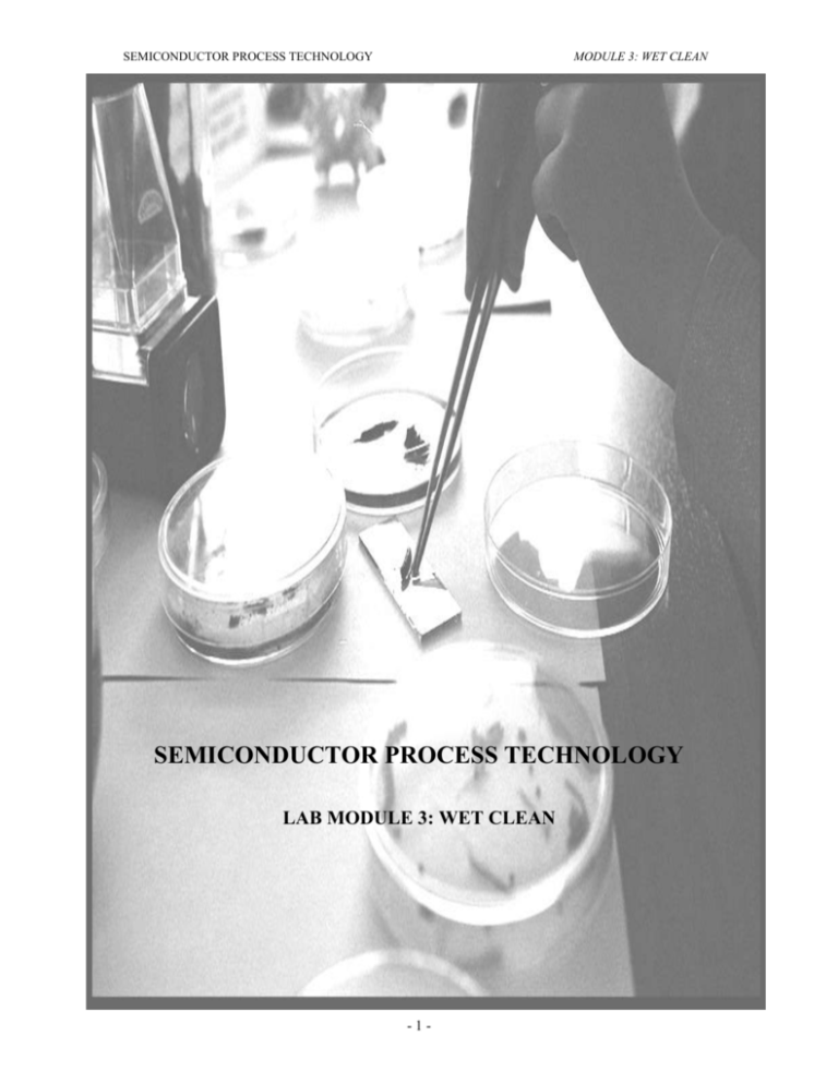
SEMICONDUCTOR PROCESS TECHNOLOGY MODULE 3: WET CLEAN SEMICONDUCTOR PROCESS TECHNOLOGY LAB MODULE 3: WET CLEAN -1- SEMICONDUCTOR PROCESS TECHNOLOGY MODULE 3: WET CLEAN THEORY Introduction The Need for Wafer Cleaning The need for scrupulously clean wafers in the fabrication of microelectronic devices has been recognized since the dawn of solid-state device technology. Clean substrate surfaces are critical in VLSI/ULSI fabrication for obtaining maximum device performance, long term reliability, and high yields. Cleaning techiques are used to remove particulate and chemical impurities so that pristine surfaces can be obtained. Such techniques must be able to do this without damaging the wafer surface. Cleaning procedures should also be safe, simple, economical, and produce a minimum of enviromentally hazardous waste products. The three general categories of wafer contaminants are: 1) particulates; 2) films; and 3) trace quantities of contaminant substances in molecular or atomic form. Particulates are any bits of material present on a wafer surface that have readily defineable boundaries. As feature sizes shrink, the sizes of particulates that can cause defects also decrease. Layers of foreign material on wafer surfaces are sources of film contamination. Portion of films may, however, break loose and become particles, as often happens with photoresist residues. Metallic and ionic contaminants are often deposited during immersion of wafers in etchant or resist stripper baths, both of which may contain metal ions and traces of free metal in solution. Wafer Cleaning Process Since several classes of contamination exist, there are separate cleaning procedures required to remove them. Some cleaning procedures are effective in removing more than one class of contaminant. Both chemical cleaning procedures and particulate cleaning techniques must be employed to produce a completely clean surface. When one technique follows another, the latter steps must not re-contaminate the surface nor degrade the effectiveness of former cleaning procedures. 1. Film Contaminants Removal Wet chemical cleaning has been the standard technique used to to remove the chemically bonded films and contaminant molecules and atoms from wafer surface. The goals of chemical cleaning are defined clearly in the SIA National Technology Roadmap, which separately defines wafer surface preparation requirements for front-end-of-line (FEOL) and back-end-of-line (BEOL) processes. The FEOL is defined as the steps that begin with a starting wafer up to first metal contact etch, and BEOL is defined as all process steps from that point on. 1.1 FEOL Wet Cleaning - RCA It is assumed that wafer processed up to the end of FEOL contain only silicon, silicon dioxide, and silicon nitride on their surface prior to high-temperature processes. Consequently, up to this point, the wafer cleaning operations can utilize highly reactive chemicals that do not attack these corrosion-resistance materials. -2- SEMICONDUCTOR PROCESS TECHNOLOGY MODULE 3: WET CLEAN When bare silicon, or silicon wafer with only thermally grown oxide is chemically cleaned prior to the furnace process, a two-step cleaning procedure formulated by Kern and Puotinen at RCA is widely used (and hence is often termed the RCA Clean). The first step in the RCA is called Standard Clean-1 (SC-1). Its function is to remove organic film contamination, some metals (Au, Ag, Cu, Ni, Cd and Cr), and particles. The second step is called Standard Clean-2 (SC-2). Its function is to remove inorganic ions, alkali ions, and heavy metals. 1.2 BEOL Wet Cleaning Once metal is deposited on a wafer, the aggressive acids and alkali solutions used in the RCA clean can no longer be used (since they would rapidly attack the metal). Instead, cleaning must be done with less reactive solvents. The most commonly used solvent in BEOL cleaning is nmethyl- pyrrolidone (NMP). Such solvents are relatively expensive and their disposal costs are also quite high. 2. Photoresist Removal Photoresist must be removed following a veriety of processing steps, including: 1) etching (wet or dry); 2) ion implantation; 3) photolithography rework. The main objective in resist stripping is to insure that all the photoresist is removed as quickly as possible without attacking any underlying surface materials. In fact, no single resist stripping technique is suitable for all applications. Resist stripping techniques are thus divided into three classes: 1) inorganic strippers; 2) organic strippers; 3) dry stripping. Inorganic strippers are solutions of H2SO4 and an oxidant, heated to around 125 ºC (e.g. Piranha solution). The oxidant typially used is H2O2. It oxidizes the carbon in the resist to form Co2, which exits from the bath as a gas. Organic strippers perform resist removal by breaking down the structure of the resist layer. Dry photoresist strippers (also called plasma resist strip) is done in plasma resist-stripping tools, with oxygen being the process gas. This offers several advantages over wet resist stripping including safer operating conditions, no metal contamination, and no attack of most underlying substrate materials. 3. Particle Removal Particles are deposited on wafers as aerosols from the air or as particles present in the liquids in which wafers are immersed. The basis of their removal rests on an understanding of how such deposited particles adhere to wafer surfaces. If a solid particle wanders close enough to the vicinity of a solid surface, then van der Waals force can attract and capture it. The particle is then physisorbed on the surface. Other forces that physisorb particles include static charge on the particles, electrostatic double-layer repulsion (EDR), and capillary adhesion, but the van der Waals (VDW) force is usually the strongest. There are three methods used to remove physisorbed particles: 1) chemically assisted removal (particle dissolution, particle oxidation, and lift-off by slight etching of the surface; 2) electrical repulsion of the particle and the surface; 3) mechanical dislodgement. -3- SEMICONDUCTOR PROCESS TECHNOLOGY MODULE 3: WET CLEAN The chemically assisted particle removal techniques are implemented in some wet cleaning procedures. For example, in the SC-1 step of RCA clean, several chemically-assisted particle removal mechanisms are believed to work in tandem. That is, the SC-1 solution removes organic particles by dissolution. It removes other type of particles by slightly simultaneously oxidizing and etching the silicon surface. The SC-2 process dissolves certain types of metal particles. However, as it does not attack the oxide, it does not remove particles as well as SC-1. The mechanical removal of particles generally proceeds by momentum transfer. That is, shear force impact the particle and dislodge it by either sliding it off the surface, or by rotating it until it detaches. Mechanical particle removal techniques have traditionally involved: 1) vibrational scrubbing (ultrasonic or megasonic); and 2) a technique that combines high-pressure liquid spraying and mechanical scrubbing. 4. Rinsing and Drying After the cleaning chemicals perform their function, they must be removed from the wafer surface. This is typically done by rinsing the wafers with DI water and then drying them. Rinsing and drying also represent critical steps in the cleaning sequence since they are performed so frequently. That is, rinse tanks and dryers may become major sources of particulate contamination unless they are monitored and properly maintained. In addition, complete removal of the cleaning chemicals cannot be done by just dunking the wafers in a tank of water. Thorough rinsing requires a continuous supply of clean water to the wafer surface. The resistivity of the effluent rinse water is normally monitored, and rinsing is continued until it exhibit the 18 MΩ-cm reistivity of pure DI water. -4- SEMICONDUCTOR PROCESS TECHNOLOGY MODULE 3: WET CLEAN Experiment: Wet Cleaning Process Objective: In this experiment, student will carry out three different type of cleaning. At the end of this experiment, student shall be able: 1. To describe the purpose of wet cleaning process. 2. To observe any defects/contamination on wafer surface. Equipment / Chemicals i. Wet Bench/ Fume Hood ii. Hot Plate iii. Thermometer iv. Chemical Solution, RCA 1 v. Chemical Solution, RCA 2 vi. Buffered Oxide Etch, BOE vii. DI Water viii. Tweezer Characterization/Testing 1. Particle/defect/color inspection -5- SEMICONDUCTOR PROCESS TECHNOLOGY MODULE 3: WET CLEAN Wet Cleaning Process Flow Run Card Group: Name: Lot Number: Exp No: Orientation: Size: Resistivity: Lot Start Date: LP# Equipment Wafer Preparation 1 Thickness: Planner: Process/Recipe Time Out 1. Take on wafer. Wet Cleaning RCA 1 2 1. Prepare RCA 1 solution HP Chemical: NH4OH:H2O2: DIW Ratio: 1:1:5 2. Heat RCA 1 solution T:75C 3. Immerse the wafer into RCA 1 t: 10min 4. Prepare next solution. Wet Cleaning RCA 1 2 1. Prepare RCA 2 solution HP Chemical: HCl: H2O2: DIW Ratio: 1:1:6 2. Heat RCA 2 solution T:80C 3. Immerse the wafer into RCA 2 t: 10min 4. Rinse in DI water. t: 15s 5. Spin dry. t: 15s Wet Cleaning BOE -6- INSEP Date: Substrate Type: Start Wafer Quantity: Authorized by: Data out Remarks SEMICONDUCTOR PROCESS TECHNOLOGY 3 WB 1. Immerse the MODULE 3: WET CLEAN wafer into Buffered Oxide Etch (BOE). 2. Rinse in DI water. t: 15s 3. Spin dry. t: 15s Visual Observation 4 HOM 1. Observe the wafer. 2. Record any particle/scratches. Results and Discussion 1. Explain the principle of wet etching. 2. What is the purpose of RCA 1 cleaning? -7- SEMICONDUCTOR PROCESS TECHNOLOGY MODULE 3: WET CLEAN 3. What is the purpose of RCA 2 cleaning? 4. Explain the need of a new wafer need to be clean using Hydrofluoric acid (HF) or Buffered Oxide Etch (BOE). -8-

