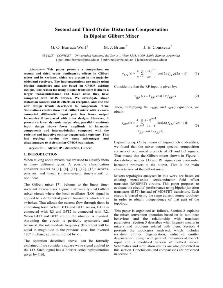
Second and Third Order Distortion Compensation in Bipolar Gilbert Mixer G. O. Barraza Wolf § M. J. Bruno † J. E. Cousseau ‡ §†‡ IIIE – CONICET – Universidad Nacional del Sur. Av. Alem 1253, 8000, Bahía Blanca, Argentina. § guillermo.barraza@uns.edu.ar † mbruno@criba.edu.ar ‡ jcousseau@uns.edu.ar Abstract−− This paper presents a comparison on second and third order nonlinearity effects in Gilbert mixer and its variants, which are present in the majority wideband receivers. The implementations are made using bipolar transistors and are based on CMOS existing designs. The reason for using bipolar transistors is due to a larger transconductance and lower noise they have compared with MOS devices. We investigate about distortion sources and its effects on reception, and also the new design trends developed to compensate them. Simulations results show that Gilbert mixer with a crossconnected differential input pair has fewer output harmonics if compared with other designs. However, it presents a lower dynamic range. Also, parallel transistors input design shows fewer amplitude in harmonic components and intermodulation compared with the resistive and inductive emitter degeneration topology. This last topology retains the same advantages and disadvantages to their similar CMOS equivalent. Keywords−− Mixer, IP3, distortion, Gilbert. 1. INTRODUCTION When talking about mixers, we are used to classify them in many different types. A possible classification considers mixers as [1], [4], [11], [12], [13]: actives, passives, and linear (time-invariant, time-variant) or nonlinear. The Gilbert mixer [7], belongs to the linear timeinvariant mixers class. Figure 1 shows a typical Gilbert mixer circuit where the local oscillator (LO) signal is applied to a differential pair of transistors which act as switches. That allows the current flow through them in alternating form. When BJT4 and BJT5 are on, BJT1 is connected with R3 and BJT2 is connected with R2. When BJT3 and BJT6 are on, the situation is inverted. Assuming the circuit is perfectly symmetric and balanced, the intermediate frequency (IF) output will be equal in magnitude to the previous case, but inverted 180º in phase, i.e., is multiplied by -1. The operation described above, can be formally explained if we consider a square wave signal applied to the LO. Such signal has a Fourier series representation given by [16]: v LO ( t ) = n −1 4 ∞ ( −1) ∑ cos[2π f LO t (2 n − 1)] π n =1 2 n − 1 (1) Considering that the RF input is given by: v RF ( t ) = VRF cos(2π f RF t ) (2) Then, multiplying the vLO(t) and vRF(t) equations, we obtain: vout ( t ) = n −1 4 ∞ ( −1) ∑ cos[2π f LO t (2 n − 1)] . π n =1 2 n − 1 (3) .V cos(2π f t ) RF RF Expanding eq. (3) by means of trigonometric identities, we found that the mixer output spectral composition consists of odd mixed products of RF and LO signals. That means that the Gilbert mixer shown in Figure 1 does deliver neither LO and RF signals nor even order harmonic products at the output. That is the main characteristic of the Gilbert mixer. Mixers topologies analysed in this work are based on existing metal-oxide semiconductor field effect transistor (MOSFET) circuits. This paper proposes to evaluate the circuits’ performance using bipolar junction transistors (BJT) instead of MOSFET transistors. Each circuit is biased using the same current source topology in order to obtain independence of that part of the topology. This paper is organized as follows. Section 2 explains the mixer conversion operation based on its nonlinear behaviour and the relationship with transistor parameters. Section 3 describes what linearity means in mixers and problems related with them. Section 4 presents the topologies analysed, which includes resistive emitter degeneration, inductive emitter degeneration, design with parallel transistors at the RF input and a modified version of Gilbert mixer. Schematics and simulation results are also presented in this section. Conclusions and comparisons are presented in section 5. 2. MIXER CONVERSION OPERATION Any mixer working as frequency converter bases its operation on a generic nonlinearity, which can be expressed as [8], [9], [14]: 2 3 i ( t ) = a + a v ( t ) + a v ( t ) + a v ( t ) + ... 0 1 2 3 (4) where i(t) is the output current, ai are coefficients of a series expansion and v(t) is the input voltage applied to the device. Eq. (4) can be analysed in more detail by giving to v(t) a voltage composed by two sinusoidal tones with frequencies ω1 and ωLO [5], [14]. Such tones can for example, represent the desired RF and LO signals going into the mixer. Consequently, v(t) can be written as: v (t ) = cos(ω1 t ) + cos(ω LO t ) (5) V_DC Replacing eq. (7) into eq. (4) and expanding, we obtain components in ± l ωLO ± k ω1 ± q ω2, where l, k and q are integers. In this case, there are a greater number of components due to the mixer nonlinearity. Since some of them will be very close the frequency band of interest they will be hard to remove by filtering. Therefore, it is necessary to take control of nonlinear mixer behavior. Depending on the technology of the device considered, eq. (4) may change to different forms. In MOSFETs transistors, the drain current signal is given by [3], [6]: ∂i i D (t ) ∂v D GS v gs (t ) + ∂i ∂v D BS v bs (t ) + ∂i ∂v D v ds where iD is drain current and vGS, vBS and vDS are gatesource, bulk-source and drain-source, voltages respectively. By associating derivative terms as transconductance factors, eq. (8) can be written as: i ( t ) gm v ( t ) + gmb v ( t ) + gds v ( t ) D gs bs ds R3 V_LOm BJT3 (9) Vout2 Vout1 V_LOp (8) DS VDC1 R2 (t ) BJT4 BJT5 V_LOp BJT6 IN_1 IN_2 BJT2 BJT1 R8 Figure 1: Classical Gilbert mixer cell. IN_1 and IN_2 are the RF inputs, V_LOp and VLOm are the LO inputs, Vout1 and Vout2 are the IF output. Replacing eq. (5) into eq. (4) produce: i ( t ) = a + a (cos(ω1 t ) + cos(ω LO t )) 0 1 2 + a (cos(ω1 t ) + cos(ω LO t )) + 2 3 a (cos(ω1 t ) + cos(ω LO t )) + ... 3 (6) Expanding eq. (6), we obtain tones in ± n ωLO ± m ω1, with n and m integers. Consequently, the output consists of a large quantity of components and only one is the desired. Therefore, will be necessary to filter out the mixer output to eliminate the unwanted signals [11]. However, the problem described above becomes more severe when several RF signals close in frequency enter to the mixer (even more when the signals are modulated). For example, consider that the mixer input consists of two RF signals (desired and interference) plus the LO signal, i.e., v ( t ) = cos(ω1 t ) + cos(ω2 t ) + cos(ω LO t ) (7) where gm and gmb are small signal gate and substrate transconductances, respectively and gds is small signal drain-source conductance. In particular, gm transconductance represents how the output current changes when the input voltage changes. In field-effect transistors (FETs) or MOSFETs, gm represents iD changes when vGS changes, which is indicated by the partial derivative in the first term on the right hand side in eq. (8). If it is required a proportional change, the iDvGS characteristic should be linear to avoid distortion. This requires that the circuit transconductance be constant in the operating range. A detailed analysis of linearized behavior of current versus bias voltage of FET transistor is given in [11]. In that case, it is assumed working on the receiver side. Therefore, the signal driven in the input circuit is assumed small enough to consider a weak nonlinearity only. Such assumption allows expanding eq. (8) into Taylor series as shown in eq. (10), where again, derivatives of order i were replaced by transconductance factors of order i [8]: i D 2 3 = gm v + gm v + gm v 1 gs 2 gs 3 gs 2 3 + gmb v + gmb v + gmb v + 1 bs 2 bs 3 bs 2 3 gds v + gds v + gds v + ... 1 ds 2 ds 3 ds (10) On doing a frequency shift, only the first term is important because it produces the sum and difference components usually employed at the mixer output. A similar analysis can be made in BJTs considering the operation at the point Q, as represented in Figure 2 [17]. iC 0.1 ic IC gm(A/V), gm2(A/V2), gm3(A/V3) 0.08 Q vbe iC ( vbe ) = I C + ic ( vbe ) (11) where IC is the DC collector current and ic is the signal collector current. Expanding eq. (11) into Taylor series, we obtain: ⎛ 1 ∂ 2iC ⎞ 2 ⎞ . v + ⎟ be ⎜ 2! 2 ⎟ .vbe ⎝ ∂v BE ⎠ ⎝ ∂v BE ⎠ (12) ⎛ 1 ∂ 3iC ⎞ 3 +⎜ 3 ⎟ .vbe + ... 3! ⎝ ∂v BE ⎠ ∂iC By associating the terms in parentheses transconductance factors, eq. (12) can be written as: i ( v ) = I + gm v + gm v C be C 1 be 2 be 2 3 + gm v + ... 3 be as (13) The factor gm1 is the first order transconductance that represents the device’s transfer characteristic slope at the point Q. A very common expression for such a factor is [17]: gm = 1 IC (14) VT where IC is the DC collector current and VT is the thermal voltage (25.2 mV at 20ºC). Therefore, the signal current can be approximated by the second term in eq. (13) as: i ( t ) gm v ( t ) = c 1 be IC VT v (t ) be 0.02 0 -0.02 0.7 0.75 0.8 0.85 0.9 vBE At the point Q, the collector current is given by: ⎛ 0.04 -0.06 Figure 2. Typical iC - vBE characteristic of a bipolar transistor. A small sinusoidal signal is superimposed on the bias voltage VBE giving rise linear operation around the bias point Q. iC ( vbe ) = I C + ⎜ gm3 0.06 -0.04 vBE VBE gm gm2 (15) Eq. (13) is similar to that found in MOSFETs. As a consequence, similar considerations about the effects of each term in the mixing can be made. Figure 3 shows the first, second and third order transconductances versus vBE for a typical bipolar transistor. As can be seen in that figure, there is a vBE value about 0.805 V for which the third order transconductance is near to zero. This is a desired operating point because it reduces an important intermodulation distortion. Figure 3. Typical characteristics of transconductance (gm), second order transconductance (gm2) and third order transconductance (gm3) of a bipolar transistor. 3. MIXER LINEARITY Linearization of a mixer refers to forcing proportionality between IF output and RF input signals. The main parameter to quantify linearity is the third-order intercept point (IP3). IP3 is a figure of merit that allows characterize the intermodulation distortion in a circuit by considering the cross point where the linear extrapolation of the fundamental signal equals the linear extrapolation of the third order harmonic [1], [2], [11]. It means a mixer is more linear when the IP3 becomes higher because less intermodulation products are generated. In general, a circuit is linear when it fulfills the superposition principle [9], [11]. Following section 2, the basic principle of the mixer is nonlinear. The linearity requirement is related to input transistors differential pair. Every time “linearity of the mixer” is mentioned, it is referred to RF inputs. The LO signal is only necessary for frequency shifting but actually it is not desired at the output. As mentioned before, mixer linearity is related to the amount of spurious products generated at the output. Ideal Gilbert mixer is a symmetric circuit which does not produce components of second order to the output. However, any difference in the symmetry of the circuit causes second order intermodulation distortion (IMD2) due to unbalanced currents that reach the load. Other nonlinearity to have in mind is that of third order which is the most important. It is responsible for the third order intermodulation distortion (IMD3) caused by the RF input transistors. A minor contribution to IMD3 is the commutation of upper differential pairs. Some techniques compensate third order transconductance (gm3) by combining similar transistors in parallel using slightly different biases. Using that technique is possible to cancel gm3 in the proximity of vBE considering BJTs or vGS considering MOSFETs. Other techniques employ -60 -90 -120 -150 3.0 2.9 2.8 2.7 2.6 2.5 2.4 2.3 2.2 2.1 2.0 1.9 1.8 1.7 1.6 1.5 1.4 1.3 1.2 1.1 1.0 0.9 0.8 0.7 0.6 0.5 0.4 0.3 0.2 0.1 0.0 With reference to circuits, the linearity allows to operate with large dynamic range signals, something that in modern communication standards is used frequently, without introduce significantly distortion at the output. 0 -30 IF_spectrum pre-distortion on the RF signal to compensate nonlinearities [18]. freq, GHz (b) -5 Conversion Gain 4. COMPENSATION TECHNIQUES PERFORMANCE All circuits were made in Agilent’s ADS (Advanced Design System) software at ωRF = 2.4 GHz, ωLO = 2.45 GHz and ωIF = 50 MHz. Each technique was evaluated using IHP’s SG25 library devices. For each topology, it is simulated the output power at the IF port showing the 1dB compression point to determine the linear operation limit. The conversion gain is also plotted as a function of RF power to analyze how the modifications change the performance gain. Finally, the output spectrum is simulated to evaluate the linearization effects on the harmonics and IMD products. R8 R10 Vout2 R9 R22 BJT5 V_LOm BJT6 R21 IN_1 BJT8 R20 BJT3 BJT4 -9 -10 -25 -20 -15 -10 -5 P_RF (c) Pideal_IF_Down PIF_DwnConv_dBm -10 -15 -20 -25 -30 -35 -30 Vout1 BJT7 -8 -40 It is the classic Gilbert mixer configuration which includes resistors at the emitter of input differential pair. The objective is to introduce some feedback in the lower differential pair aiming to increase linearity, as shown in Figure 4(a). However, the feedback disadvantages are gain loss and increased noise [4]. Figure 4(b) shows the IF spectrum, which has components very close to the desired output frequency (50 MHz). In part (c) of Figure 4 is plotted the conversion gain versus input power. We can see the gain is nearly constant for small level inputs (lower than -20 dB). Figure 4(d) shows the output power response to expose the mixer nonlinear behaviour as a function of input power. The vertical line indicates the 1 dB compression point to emphasize the point where the fundamental output curve is 1 dB lower than predicted by the ideal output curve. R7 -7 -11 -30 4.1. Resistive emitter degeneration -25 -20 -15 -10 -5 P_RF (d) Figure 4. (a) Gilbert mixer with emitter resistor degeneration (SRL1 = 20 Ω, 0 nH). (b) IF output spectrum. (c) Conversion gain vs. RF power: P_RF 1dB: -14.9 dBm, Gain 1dB: -6.3 dB. (d) IF power vs. RF power: P_IF 1dB: -21.2 dBm, P_IF ideal: -20.2 dBm. 4.2. Inductive emitter degeneration It is the same configuration that in Figure 4(a) but considering RS = 0 and LS = 1.3 nH. The advantage of replacing the resistor by an inductor consists in the little voltage drop in the inductor due to current bias, which is important if the design must work at low voltage. However, the main disadvantage of inductive degeneration is the operation of the design, which will depend on the frequency. The results are shown in Figure 5. In part (a) of that figure, is shown the output spectrum. If compared with Figure 4(b), it can be seen a reduction in the first spectral line close to the fundamental output at 50 MHz. Figure 5(b) shows that the conversion gain is reduced for about 1.2 dB at the 1 dB compression point compared with the mixer with emitter resistor degeneration. In Figure 5(c), the output power versus input power is shown. The output power at the 1 dB compression point is -20.9 dBm, which is 0.3 dBm greater than the previous circuit. p SRL1 p 0 IN_2 -30 BJT2 IF_spectrum V_LOp m1 -6 BJT1 -60 -90 -120 R19 R18 -150 3.0 2.9 2.8 2.7 2.6 2.5 2.4 2.3 2.2 2.1 2.0 1.9 1.8 1.7 1.6 1.5 1.4 1.3 1.2 1.1 1.0 0.9 0.8 0.7 0.6 0.5 0.4 0.3 0.2 0.1 0.0 freq, GHz (a) (a) 0 m1 -30 IF_spectrum Conversion Gain -4 -6 -8 -60 -90 -120 -10 -150 3.0 2.9 2.8 2.7 2.6 2.5 2.4 2.3 2.2 2.1 2.0 1.9 1.8 1.7 1.6 1.5 1.4 1.3 1.2 1.1 1.0 0.9 0.8 0.7 0.6 0.5 0.4 0.3 0.2 0.1 0.0 -12 -30 -25 -20 -15 -10 freq, GHz -5 (b) P_RF (b) Conversion Gain -10 Pideal_IF_Down PIF_DwnConv_dBm -5 m3 -15 -20 -25 m1 -6 -7 -8 -9 -10 -11 -30 -30 -25 -35 -30 -25 -20 -15 -10 -5 R10 R8 Vout1 Vout2 R9 R22 BJT6 BJT8 Pideal_IF_Down PIF_DwnConv_dBm -20 -25 -30 -35 -40 -25 -20 -15 -10 -5 P_RF This is a modification made in [15]. The focus is linearizing the third order transconductance by reducing its negative peak with the positive peak of the third order transconductance of another transistor in parallel with the first. The circuit and simulations are shown in Figure 6. V_LOm -15 -30 4.3. Design with Parallel transistors at the RF input BJT5 -5 (c) Figure 5. Simulations results for Gilbert mixer with inductive emitter degeneration (SRL1 = 0 Ω, 1.3 nH). (a) IF output spectrum. (b) Conversion gain vs. RF power: P_RF 1dB: -15.8 dBm, Gain 1dB: -5.1 dB. (c) IF power vs. RF power: P_IF 1dB: -20.9 dBm, P_IF ideal: -19.9 dBm. BJT7 -10 -10 (c) R7 -15 P_RF P_RF V_LOp -20 (d) Figure 6: (a) Gilbert mixer with parallel transistors at input. (b) IF output spectrum. (c) Conversion gain vs. RF power: P_RF 1dB: -13.4 dBm, Gain 1dB: -6.7 dB. (d) IF power vs. RF power: P_IF 1dB: -20.1 dBm, P_IF ideal: -19.1 dBm. Figure 6(b) shows the spectral output where it can be appreciated a greater reduction in the first spectral line compared with the mixer with inductive emitter degeneration and also a reduction in the harmonics levels at 2.4 GHz and 2.5 GHz. Figure 6(c) shows that the conversion gain is -6.7 dB, 0.4 dB lower than the resistive emitter degeneration and 1.6 dB lower than the inductive emitter degeneration. However, as shown in Figure 6(d), the input power level at the compression point is higher, which means the input dynamic range is also higher. 4.4. Modified Gilbert mixer R21 R20 IN_1 BJT15 BJT3 BJT4 SRL1 BJT16 IN_2 BJT2 BJT1 R19 R18 (a) It is the modification made in [10] for MOSFETs and adapted here to BJT design, as shown in Figure 7. In this case, the idea is to employ the same configuration used at the LO input but at the RF input. Simulation results show in Figure 7(b) the output spectrum is greatly reduced. It can be seen the spectral line at 100 MHz has disappeared as well as the harmonics at 2.4 GHz and 2.5 GHz. However, these benefits are at the expense of conversion gain, as shown in Figure 7(c). Finally, in Figure 7(d) is appreciated that the input power at the 1dB compression point is the lower of all considered. R10 R8 Vout1 Vout2 R9 R7 R22 V_LOp BJT7 BJT8 BJT9 V_LOm BJT10 R21 R20 R24 distortion at the output despite the fact that they are working as commutation devices. However, they are responsible of generation of multiple RF and LO odd harmonics at the output in the GHz range. This does not affect the system linearity because they may be filtered out. Using quadratic law devices such as FETs instead of bipolar transistors may help to reduce spurious effects at the output. As a future work, it is proposed to combine BJTs and MOSFETs in a same mixer circuit with the purpose of evaluating the characteristics and performance. IN_1 BJT3 BJT4 BJT5 REFERENCES BJT6 IN_2 BJT2 BJT1 R19 R18 (a) 0 IF_spectrum -30 -60 -90 -120 -150 3.0 2.9 2.8 2.7 2.6 2.5 2.4 2.3 2.2 2.1 2.0 1.9 1.8 1.7 1.6 1.5 1.4 1.3 1.2 1.1 1.0 0.9 0.8 0.7 0.6 0.5 0.4 0.3 0.2 0.1 0.0 freq, GHz (b) Conversion Gain -6 m1 -8 -10 -12 -14 -30 -25 -20 -15 -10 -5 P_RF (c) Pideal_IF_Down PIF_DwnConv_dBm -10 3 -15 -20 -25 -30 -35 -40 -30 -25 -20 -15 -10 -5 P_RF (d) Figure 7: (a) Gilbert mixer modified. (b) IF output spectrum. (c) Conversion gain vs. RF power: P_RF 1dB: P_RF 1dB: -16.9 dBm, Gain 1dB: -7.7 dB. (d) IF power vs. RF power: P_IF 1dB: -24.6 dBm, P_IF ideal: -23.6 dBm. 5. CONCLUSIONS Gilbert mixer commutation linearity is mainly affected by the transconductance of RF input differential pair. The transistors of the upper differential pair where the LO signal is applied, do not introduce a large IM [1] Lee, “The Design of CMOS Radio-Frequency Integrated Circuits”, Cambridge University Press, 1998 (chapter 4). [2] Ding, “High Linearity CMOS RF Front-end Circuits”. [3] Tsividis, “Mixed Analog-Digital VLSI Devices and Technology”, 2005 (pp. 30-49). [4] Gilmore, “Practical RF Circuit Design for Modern Wireless Systems Volume II, Active Circuits and Systems” (pp. 440-442, 485, 487). [5] Gilmore, “Practical RF Circuit Design For Modern Wireless Systems Volume I, Passive Circuits and Systems” (pp. 100-109). [6] Cressler, “Circuits and Applications Using Silicon Heterostructure Devices”, CRC Press, 2008. [7] Gilbert, “A Precise Four-Quadrant Multiplier with Subnanosecod Response”, IEEE Journal of SolidState Circuits, VOL. SC-3, NO. 4, December 1968. [8] Kang, “Linearity Analysis of CMOS for RF Application”. [9] Kivekas, “Design and Characterization of Downconversion Mixers and the On-chip Calibration Techniques for Monolithic Direct Conversion Radio Receivers. [10] Mitrea, “A Linearization Technique for Radio Frequency CMOS Gilbert-Type Mixers”. [11] Pedro, “Intermodulation Distortion in Microwave and Wireless Circuits”, Artech House, 2003, (pp. 56, 213-251 y 305). [12] ARRL, “The ARRL Handbook for Radio Communications”, 2007. [13] Yongwang Ding, “High Linearity CMOS RF Front-End Circuits”. [14] Long, “Fundamentals of Mixer Design”, Agilent Technologies, 2001. [15] Kim, “Highly Linear Receiver Front-End Adopting MOSFET Transconductance Linearization”. [16] Haykin, “Communication Systems”, Wiley, 1983. [17] Sedra, Smith, “Microelectronic Circuits”, Oxford University Press, 1998. [18] Yang, “A 2.4GHz Low Power Highly Linear Mixer for Direct-Conversion Receivers”.


