Tutorial-3: Mixer Design
advertisement
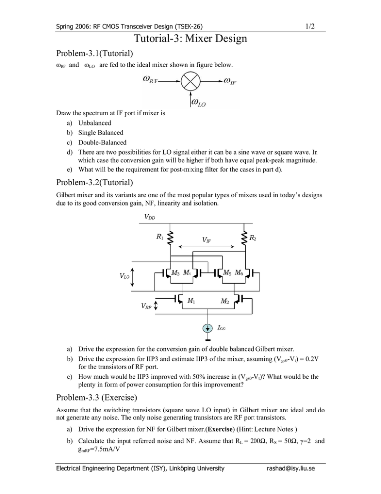
1/2 Spring 2006: RF CMOS Transceiver Design (TSEK-26) Tutorial-3: Mixer Design Problem-3.1(Tutorial) ωRF and ωLO are fed to the ideal mixer shown in figure below. Draw the spectrum at IF port if mixer is a) Unbalanced b) Single Balanced c) Double-Balanced d) There are two possibilities for LO signal either it can be a sine wave or square wave. In which case the conversion gain will be higher if both have equal peak-peak magnitude. e) What will be the requirement for post-mixing filter for the cases in part d). Problem-3.2(Tutorial) Gilbert mixer and its variants are one of the most popular types of mixers used in today’s designs due to its good conversion gain, NF, linearity and isolation. VDD R1 M3 M4 VLO VRF R2 VIF M1 M5 M6 M2 ISS a) Drive the expression for the conversion gain of double balanced Gilbert mixer. b) Drive the expression for IIP3 and estimate IIP3 of the mixer, assuming (Vgs0-Vt) = 0.2V for the transistors of RF port. c) How much would be IIP3 improved with 50% increase in (Vgs0-Vt)? What would be the plenty in form of power consumption for this improvement? Problem-3.3 (Exercise) Assume that the switching transistors (square wave LO input) in Gilbert mixer are ideal and do not generate any noise. The only noise generating transistors are RF port transistors. a) Drive the expression for NF for Gilbert mixer.(Exercise) (Hint: Lecture Notes ) b) Calculate the input referred noise and NF. Assume that RL = 200Ω, RS = 50Ω, γ=2 and gmRF=7.5mA/V Electrical Engineering Department (ISY), Linköping University rashad@isy.liu.se 2/2 Spring 2006: RF CMOS Transceiver Design (TSEK-26) Problem-3.4 (Tutorial) Passive mixers have better IM3 performance but higher conversion loss and hence higher noise figures compared to active mixers. A double balanced passive mixer is shown with square wave oscillator VLO(t). Assume that VRF(t)= ARF Cos(ωRFt). RS/2 + - LO Vout LO LO RS LO VRF RS/2 a) Find the conversion gain of mixer in dB if the switches are ideal. b) Find the conversion gain of mixer in dB if the switches have on resistance of Rs/2. c) Derive the expression for the device width if the maximum gain degradation is no more than 1 dB compared to the gain in part a). Assume that the transistor is working in linear region. d) Drive the expression for total power consumed by LO in driving the capacitance of all transistors working as switch. e) What happens when the LO duty cycle is not 50%, draw the approximate frequency plot to motivate your answer. (Exercise) Problem-3.5 (Home Work) Design a differential input stage (RF stage) of CMOS Gilbert mixer. The mixer should meet following specifications IIP3=10dBm, NF= 10dB. Assume Kn = 100uA/V2, RL = 200Ω, RS = 50Ω and γ=2. Electrical Engineering Department (ISY), Linköping University rashad@isy.liu.se

