the Cause of Excess Current in Superconducting Tunnel Junctions?
advertisement
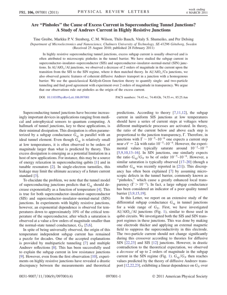
PRL 106, 097001 (2011) PHYSICAL REVIEW LETTERS week ending 4 MARCH 2011 Are ‘‘Pinholes’’ the Cause of Excess Current in Superconducting Tunnel Junctions? A Study of Andreev Current in Highly Resistive Junctions Tine Greibe, Markku P. V. Stenberg, C. M. Wilson, Thilo Bauch, Vitaly S. Shumeiko, and Per Delsing Department of Microelectronics and Nanoscience, Chalmers University of Technology, SE-41296 Göteborg, Sweden (Received 25 August 2010; published 28 February 2011) In highly resistive superconducting tunnel junctions, excess subgap current is usually observed and is often attributed to microscopic pinholes in the tunnel barrier. We have studied the subgap current in superconductor–insulator–superconductor (SIS) and superconductor–insulator–normal-metal (SIN) junctions. In Al=AlOx =Al junctions, we observed a decrease of 2 orders of magnitude in the current upon the transition from the SIS to the SIN regime, where it then matched theory. In Al=AlOx =Cu junctions, we also observed generic features of coherent diffusive Andreev transport in a junction with a homogenous barrier. We use the quasiclassical Keldysh-Green function theory to quantify single- and two-particle tunneling and find good agreement with experiment over 2 orders of magnitude in transparency. We argue that our observations rule out pinholes as the origin of the excess current. DOI: 10.1103/PhysRevLett.106.097001 PACS numbers: 74.45.+c, 74.40.Gh, 74.55.+v, 85.25.Am Superconducting tunnel junctions have become increasingly important devices in applications ranging from medical and astrophysical sensors to quantum computing. A hallmark of tunnel junctions, key to these applications, is their minimal dissipation. This dissipation is often parameterized by a subgap conductance Gsg in parallel with an ideal tunnel element. Even though Gsg is relatively small at low temperatures, it is often observed to be orders of magnitude larger than what is predicted by theory. This excess dissipation is emerging as a potential limitation in a host of new applications. For instance, this may be a source of energy relaxation in superconducting qubits [1] and in tunable resonators [2]. In single-electron turnstiles, this leakage may limit the ultimate accuracy of a future current standard [3]. To elucidate the problem, we note that the tunnel model of superconducting junctions predicts that Gsg should decrease exponentially as a function of temperature [4]. This is true for both superconductor–insulator–superconductor (SIS) and superconductor–insulator–normal-metal (SIN) junctions. In experiments with highly resistive junctions, however, an exponential dependence is observed for temperatures down to approximately 10% of the critical temperature of the superconductor, after which a saturation is observed at a value a few orders of magnitude smaller than the normal-state tunnel conductance, GN [5,6]. In spite of being universally observed, the origin of this temperature independent subgap current has remained a puzzle for decades. One of the accepted explanations is provided by multiparticle tunneling [7] and multiple Andreev reflections [8]. This has been successfully used to explain the subgap current in low resistance junctions [9]. However, even from the first observation [10], experiments on highly resistive junctions have revealed a drastic discrepancy between the measurements and theoretical 0031-9007=11=106(9)=097001(4) predictions. According to theory [7,11,12], the subgap current in uniform SIS junctions at low temperatures should have a series of current steps at voltages where different multiparticle processes are activated. In theory, the ratio of the current below and above each step is proportional to the junction transparency, . Therefore, in junctions with 105 –106 one expects a current step near eV ¼ 2 with ratio 105 –106 . However, the experimental values typically saturate around 102 –103 [5,9,10,13–16]. In SIN junctions, one similarly expects the ratio Gsg =GN to be of order 105 –106 . However, a similar saturation is typically observed [17–20] (though a smaller Gsg was recently reported in [21]). This discrepancy has often been explained [7] by assuming microscopic defects in the tunnel barrier, commonly known as ‘‘pinholes,’’ which cause a greatly enhanced local transparency ( > 103 ). In fact, a large subgap conductance has been considered an indicator of a poor quality tunnel barrier [3,9,15,19]. In this Letter, we report on an extensive study of the differential subgap conductance Gsg in tunnel junctions for a wide range of GN . First, we have investigated Al=AlOx =Al junctions (Fig. 1), similar to those used in qubit circuits. We investigated both the SIS and SIN transport regimes in these junctions. This was done by making one electrode thicker and applying an external magnetic field to suppress the superconductivity in this electrode. The two-particle current should not change significantly during this crossover according to theories for diffusive SIN [22,23] and SIS [12] junctions. However, in drastic contradiction to the theoretical expectation, we observed a decrease of up to 2 orders of magnitude in the subgap current in the SIN regime (Fig. 1). Gsg =GN then reaches values predicted by the theory of diffusive Andreev transport [12,22,23], exhibiting a linear dependence on GN over 097001-1 Ó 2011 American Physical Society PRL 106, 097001 (2011) PHYSICAL REVIEW LETTERS overlap width 200 nm FIG. 1 (color online). I-V characteristics of two typical lowtransparency Al=AlOx =Al junctions (red and black) at T < 100 mK. In the SIS regime (left, B ¼ 0 mT), a step is observed with the ratio of currents below and above eV ¼ 2 being 2 103 , consistent with previously published work. However, the subgap current is strongly suppressed upon the transition from the SIS to the SIN regime (right, B > 300 mT) and approaches the theoretically predicted limit. The inset shows an electron micrograph of the junction. more than 2 orders of magnitude. We ultimately achieve Gsg =GN 105 (Fig. 2). To corroborate that we reached the fundamental limit for Gsg set by Andreev reflection, we fabricated and investigated generic SIN Al=AlOx =Cu junctions. Here we achieved similarly small values of Gsg , as shown in Fig. 2. Moreover, we observed a zero-bias conductance peak (ZBCP), a fingerprint of coherent diffusive Andreev transport [22–25]. This peak is suppressed by magnetic field and thus was not observed in the all-Al junctions. We further measured a dependence of Gsg on the effective electronic mean free path in the electrodes. As we will show, these observations indicate homogeneity of the tunnel barriers on the spatial scale of the mean free path. Our junctions were fabricated on oxidized Si substrates by the standard Dolan evaporation technique with in situ FIG. 2 (color online). Ratios Gsg;min =GN versus normal conductance per geometric area GN =A in SIN junctions; experimental points are indicated with dots and triangles, the lines show theoretical predictions of Eq. (1). Inset: For a fixed GN , we observe that Gsg;min is inversely proportional to A, thus exhibiting a linear dependency on as suggested by Eq. (1). week ending 4 MARCH 2011 thermal growth of aluminum oxide. Both metal leads are evaporated resistively at a base pressure of 106 mbar with a 0:5–1 nm=s evaporation rate. The junctions were e-beam patterned using a two or three layer resist system. The Al=AlOx =Al junctions were 100–400 nm wide with an overlap of 400 nm [Fig. 1(a)]. A variation of the oxygen dose (the product of pressure and time) from 17 mbar s to 8 bar s yielded RN values from 0.2 to 13 k. The Al=AlOx =Cu junctions were 80 nm wide with an overlap of 220 nm. A variation of the dose from 1.9 to 120 bar s yielded RN values from 1.5 to 200 k. We note that the growth conditions for the base electrode and barrier are the same in both types of devices. We therefore assume that the barrier qualities are similar in both. The junctions were measured in a dilution refrigerator at temperatures below 100 mK. Each dc line was equipped with a two-stage RLC filter, a powder filter, and with 2 m of thermocoax cable. The junctions were voltage biased and the current was read out either through a bias resistor or a transimpedance amplifier. The former method introduced excess noise for the high-RN junctions which is why the latter method was used for these junctions. To understand the experimental data, we applied a theory of the superconducting proximity effect based on quasiclassical Keldysh-Green function techniques [22,23]. Both single- and two-particle processes contribute to the subgap conductance. The single-particle contribution is given by the conventional tunnel model [4]. The twoparticle Andreev conductance is given by 3 Z dE pffiffiffiffiffiffiffiffiffiffiffiffiffiffiffiffiffiffi 2 4l 0 E2 s ffiffiffiffiffiffiffiffi sffiffiffiffiffiffiffiffiffiffiffiffi D E tanh Re @ f ðE; VÞ: (1) 2iE 2iETh V N GA ðVÞ ¼ GN Here fN ðE; VÞ ¼ ð1=2Þftanh½ðE þ eVÞ=2kB T tanh ½ðE eVÞ=2kB Tg and ETh ¼ @D=L2 is the Thouless energy with D the diffusion constant, l the mean free path, and L the length of the normal electrode. Equation (1) is valid in the experimentally relevant limit of phase-coherent diffusive transport over the distance L l and assuming that GN is significantly smaller than the conductance of the normal lead. Furthermore, it is assumed that ETh . Important features of the Andreev conductance (1) which are relevant for interpretation of the experiment are (i) the presence of an additional factor indicating the two-particle origin of the Andreev transport, (ii) the enhanced value at zero voltage, GA ð0Þ ¼ GN ð3L=4lÞ (ZBCP), and (iii) the dependence on l. The ZBCP is indicative of the coherent, diffusive transport regime. It is explained by an electron-hole transmission resonance formed by the interplay between Andreev reflection and scattering by impurities [23,25]. The resonance is destroyed by an external magnetic field B, and the 097001-2 PRL 106, 097001 (2011) PHYSICAL REVIEW LETTERS ZBCP disappears according pffiffiffito GA ðV ¼ 0; BÞ ¼ GA ðV ¼ 0Þ tanhðbÞ=b, where b ¼ 2L LeB=@, and L is the London penetration length [22]. The ZBCP is usually observed in high-transparency SIN junctions based on two-dimensional electron gases [24], though it has also been found in metallic junctions with intermediate transparencies [17,20]. Other transport characteristics of diffusive SIN junctions, e.g., shot noise, also exhibit a zero-bias anomaly [26]. Figure 2 shows the measured ratios Gsg;min =GN for a wide range of barrier thicknesses in Al=AlOx =Al and Al=AlOx =Cu junctions measured in the SIN regime. Here Gsg;min indicates the minimum value of Gsg approximately at eV =2. The conductance per unit area, GN =A, where A is the junction area, was varied over more than 2 orders of magnitude. The measured ratios Gsg;min =GN are proportional to GN =A as the theory (red and black lines) predicts, down to the lowest values measured 105 . At a fixed GN , we observe that Gsg;min is inversely proportional to A, indicating a linear dependence on (inset of Fig. 2). Gsg vs voltage characteristics have been investigated in detail in all measured Al=AlOx =Cu junctions. Figure 3 shows curves for two junctions, with parameters, GN ¼ 50 S, ¼ 2 105 (red solid), and GN ¼ 300 S, ¼ 1 104 (blue solid). In order to fit GN and the one- and two- particle contributions to Gsg simultaneously, one must make assumptions about the distribution of for the many microscopic conduction channels in the junction. We use a FIG. 3 (color online). (a) Subgap conductance vs voltage measured in SIN tunnel junctions with transparencies ¼ 1 104 (blue, right y-axis) and ¼ 2 105 (red, left y-axis), solid lines. The best fit (dashed lines) is obtained by adding the singleparticle conductance to GA ðVÞ of Eq. (1) (dash-dotted lines), assuming an electronic temperature of 100 mK, and finite values of the Dynes parameter (defined in the text), ¼ 4 105 and ¼ 4 104 , respectively. (b) Suppression of ZBCP by magnetic field B applied parallel to the substrate. Dots are experimental data. The line is theory. Inset shows GðVÞ curves for fields: B ¼ 0; 180 mT; 280 mT (from top to bottom). week ending 4 MARCH 2011 minimal model of a uniform in an active area which may be smaller than the geometric area. We find that the active area is about 13% of the geometric area (cf. [17]). The other parameters used for the theoretical fitting are ¼ 210 eV, DCu ¼ 130 cm2 =s, and LCu ¼ 5 m. The best fit is achieved assuming an electronic temperature of 100 mK (the cryostat temperatures were 70 and 40 mK, respectively), and a tunneling density of states that is broadened due to spurious inelastic processes. The broadening is parameterized by adding a small imaginary part to the quasiparticle energy, E þ i (the Dynes parameter [21,27]), having values of ¼ 4 105 and ¼ 4 104 , respectively. Note that affects the single-particle conductance but not GA . We found similar values of temperature and values of the same order for all junctions that were fit. We also measured the effect of an applied magnetic field on the ZBCP. The results [Fig. 3(b)] are in a good quantitative agreement with the theory. The ZBCP disappears in magnetic fields larger than 280 mT, even while the Al electrode remains superconducting. To verify the dependence of the subgap conductance on the mean free path, we fabricated junctions with different thicknesses d of the Cu layer. In bare Cu wires, resistivity as a function of d exhibited a crossover from a constant to a 1=d dependence at d 50 nm [Fig. 4(a)], suggesting a crossover to surface dominated electron scattering. Figures 4(b) and 4(c) show measurements of Rsg vs d. Each point is the average of several junctions. At approximately the same thickness, d < 50 nm, the data exhibit a FIG. 4 (color online). Scaling of the transport characteristics with thickness of the Cu electrode d: (a) specific resistance of the Cu electrode, (b) normalized zero-voltage resistance, and (c) normalized maximum value of resistance. Dots correspond to averages over several measured junctions, the error bars denote the standard deviation. Dashed lines show asymptotic behaviors extracted from Eq. (1). 097001-3 PRL 106, 097001 (2011) PHYSICAL REVIEW LETTERS crossover from constant behavior to a variation consistent pffiffiffi with Eq. (1), namely Rsg ðV ¼ 0Þ / d and Rsg;max / d. From the measured dependence of Gsg on electrode thickness, we can draw important conclusions about the uniformity of our tunnel barriers. The employed theoretical model assumes a homogeneous tunnel barrier on the scale of l. The fact that our observations agree with this model implies that any inhomogeneity of the tunnel barrier has a spatial scale larger than 50 nm. If subgap transport were dominated by pinholes with a smaller size, the current would rapidly spread out in the electrode, so that electron scattering would not play a role, and transport would resemble that of a ballistic constriction. In that case, Gsg would not show any dependence on d. We note that this 50 nm size scale matches that of the metallic grains in our base electrodes. This suggests a picture where the tunnel barrier is uniform on any given grain, but varies from grain to grain. The active tunneling area we extract then corresponds to a couple of grains. Having concluded that the tunnel barriers in our devices do not have pinholes, we must therefore conclude that the greatly enhanced subgap current when one-and-the-same device is measured in the SIS regime cannot be attributed to pinholes. It must be caused by other mechanisms, e.g., environmental resonances [28], and it remains an open question. It is reasonable to extend this conclusion to other junctions fabricated using similar fabrication techniques, which are in fact quite common. We note that has implications for decoherence in superconducting qubits. In SIS junctions, it gives a residual conductance, GðV ¼ 0Þ ¼ GN =, which should lead to relaxation. Considering, e.g., a transmon qubit, we obtain a relaxation time T1 ¼ 2 =@!2 . Observed values of T1 6:5 s [29] would imply = 104 , similar to our results, although this is not proof of causation. In conclusion, we have demonstrated a decrease of subgap current by 2 orders of magnitude in tunnel junctions as one of the superconducting electrodes is made normal. Good quantitative agreement with theory was observed in SIN junctions over a span of more than 2 orders of magnitude of the junction transparencies, 104 –106 , with a minimum value of Gsg =GN 105 . We observed all the generic features of coherent diffusive Andreev transport. Taken together, these observations strongly suggest that highly transparent, microscopic pinholes in the tunnel barrier are not the explanation for the observed excess subgap current in highly resistive SIS tunnel junctions. This research was partly funded by the Office of the Director of National Intelligence (ODNI), Intelligence Advanced Research Projects Activity (IARPA), through the Army Research Office. All statements of fact, opinion or conclusions contained herein are those of the authors week ending 4 MARCH 2011 and should not be construed as representing the official views or policies of IARPA, the ODNI, or the U.S. Government. We also acknowledge the Swedish Research Council (VR) and the Wallenberg Foundation for support. [1] Y. Makhlin, G. Schön, and A. Shnirman, Rev. Mod. Phys. 73, 357 (2001). [2] M. Sandberg et al., Appl. Phys. Lett. 92, 203501 (2008). [3] J. P. Pekola et al., Nature Phys. 4, 120 (2007). [4] A. Barone and G. Paternò, Physics and Applications of the Josephson Effect (Wiley, New York, 1982). [5] M. A. Gubrud et al., IEEE Trans. Appl. Supercond. 11, 1002 (2001). [6] A. W. Kleinsasser, F. M. Rammo, and M. Bhushan, Appl. Phys. Lett. 62, 1017 (1993). [7] J. R. Schrieffer and J. W. Wilkins, Phys. Rev. Lett. 10, 17 (1963). [8] T. M. Klapwijk, G. E. Blonder, and M. Tinkham, Physica (Amsterdam) 109–110B+C, 1657 (1982). [9] A. W. Kleinsasser et al., IEEE Trans. Appl. Supercond. 5, 2735 (1995). [10] B. N. Taylor and E. Burstein, Phys. Rev. Lett. 10, 14 (1963). [11] E. N. Bratus’, V. S. Shumeiko, and G. Wendin, Phys. Rev. Lett. 74, 2110 (1995). [12] E. V. Bezuglyi et al., Phys. Rev. B 73, 220506 (2006). [13] K. M. Lang et al., IEEE Trans. Appl. Supercond. 13, 989 (2003). [14] F. P. Milliken et al., Appl. Phys. Lett. 85, 5941 (2004). [15] S. Oh et al., Supercond. Sci. Technol. 18, 1396 (2005). [16] M. G. Castellano et al., Supercond. Sci. Technol. 19, 860 (2006). [17] H. Pothier et al., Phys. Rev. Lett. 73, 2488 (1994). [18] D. Quirion et al., Phys. Rev. B 65, 100508 (2002). [19] S. V. Lotkhov et al., Physica (Amsterdam) 449C, 81 (2006). [20] S. Rajauria et al., Phys. Rev. Lett. 100, 207002 (2008). [21] J. P. Pekola et al., Phys. Rev. Lett. 105, 026803 (2010). [22] A. F. Volkov and T. M. Klapwijk, Phys. Lett. A 168, 217 (1992); A. F. Volkov, Phys. Lett. A 174, 144 (1993); A. F. Volkov, A. V. Zaitsev, and T. M. Klapwijk, Physica (Amsterdam) 210C, 21 (1993); A. F. Volkov, Physica (Amsterdam) 203B, 267 (1994). [23] F. W. J. Hekking and Y. V. Nazarov, Phys. Rev. B 49, 6847 (1994). [24] A. Kastalsky et al., Phys. Rev. Lett. 67, 3026 (1991). [25] B. J. van Wees et al., Phys. Rev. Lett. 69, 510 (1992). [26] M. P. V. Stenberg and T. T. Heikkilä, Phys. Rev. B 66, 144504 (2002). [27] R. C. Dynes et al., Phys. Rev. Lett. 53, 2437 (1984). [28] T. Greibe et al., J. Phys. Conf. Ser. 150, 052063 (2009). [29] A. A. Houck et al., Phys. Rev. Lett. 101, 080502 (2008). 097001-4

