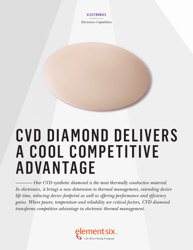
CVD diamond thermal management
advertisement

E L E C T R O NI C S Electronics Capabilities CVD DIAMOND DELIVERS A COOL COMPETITIVE ADVANTAGE ———– Our CVD synthetic diamond is the most thermally conductive material. In electronics, it brings a new dimension to thermal management, extending device life time, reducing device footprint as well as offering performance and efficiency gains. Where power, temperature and reliability are critical factors, CVD diamond transforms competitive advantage in electronic thermal management. INCRE ASE PERFORMANCE, EFFICIENCY AND DE V ICE LIFE TIME – Leveraging synthetic diamond’s unparalleled thermal properties allows semiconductor design engineers to address today’s critical challenges such as improved reliability and increased power density on a smaller footprint, thereby delivering worldleading competitive advantage to both device and system manufacturers alike. ELEMENT SIX CVD DIAMOND EXPERTISE OPTIMIZES C U S T O M E R I M P L E M E N TAT I O N CVD diamond can be made with thicknesses from 100 to 2000 microns and in diameters up to 140 mm. Laser cutting and polishing capabilities provide our customers the geometries, surface flatness and low roughness to meet their specific requirements. Our metallization expertise gives our customers a functional material they can use in die bonding with low thermal barrier resistances. – Combining low weight, electrical insulation, mechanical strength, low toxicity and low dielectric constant with a room-temperature thermal conductivity up to 5 times higher than copper makes microwave CVD diamond the optimal heat spreader material for device and package designers. T Y PIC A L PACK AGE GEOME T RY W I T H C V D DI A MOND MOUN T ED IN MODUL E – Using over 25 years of experience, Element Six tailors diamond properties to meet its customers’ specific performance/ cost requirements and custom cuts and metalizes diamond to help customers integrate singulated heat spreaders into their modules and systems. Hot spot TIM1 - primary interface CVD Diamond Heat Spreader – CVD diamond enables dramatic increases in lifetime and/ or power and reduced operating costs for the latest semiconductor GaN devices. General heat flow direction Heat Sink Package T R A N S F ORMING T HERM A L M A N AGEMEN T PER F OR M A NCE H I G H E S T R O O M -T E M P E R AT U R E T H E R M A L C O N D U C T I V I T Y O F A N Y M AT E R I A L T Y PIC A L A PPL IC AT ION S Heat is the single biggest cause of failure in electronics. Statistically, reducing the operating junction temperature by 10°C can double a device lifetime. CVD diamond outperforms today’s common materials for thermal management, such as copper, silicon carbide, and aluminium nitride by factors of 3 to 10 times. HIGH-POWER RF DEVICES – Base station RF amplifiers – Satellite RF uplink amplifiers – Microwave amplifiers HIGH-POWER OPTOELECTRONICS – Laser diodes and laser diode arrays – Optical planar IC modules – High-brightness LEDs T HE RM A L C ONDUC T I V I T Y H I G H V O LTA G E P O W E R D E V I C E S – – – – DIAFILM TM200 DIAFILM TM180 DIAFILM TM150 DIAFILM TM100 Cu Automotive sub systems Aerospace sub systems Energy distribution DC/DC converters SEMICONDUCTOR EQUIPMENT BeO – Characterization testing – Die-attachment processes AIN 0 500 1000 1500 T H E R M A L C O N D U C T I V I T Y ( W/ mK ) 2000 Electronics Capabilities 2 Chip or 'die' TIM2 - low melting solder R APIDLY EMERGING T ECHNOLOGY APPLICAT IONS HIGH - P O W E R R F A ND OP T OEL E C T R ONIC S S EMIC ONDUC T OR A S S EMBLY & T E S T H I G H E R P O W E R AT L O W E R O P E R AT I N G T E M P E R AT U R E L O N G E R T E S T I N G T I M E A N D E V E N LY AT TA C H E D D I E CVD enables high-power RF and optoelectronic devices to: – Run at higher power levels without increasing junction operating temperature – Run at the same power level, but much cooler, thereby increasing lifetimes and reliability – Wide optical transmission enables CVD diamond heat spreaders to operate within an optical path, such as in laser cavities, without optical performance degradation CVD diamond enables longer testing time during semiconductor device characterization by keeping them colder during stress testing and characterization. CVD diamond also ensures heat is rapidly and evenly spread across the entire semiconductor area during die attachment, ensuring strong and reliable contact. GA N - ON - DI A MOND R A P I D , E F F I C I E N T A N D C O S T- E F F E C T I V E H E AT E X T R A C T I O N C V D DI A MOND HE AT S PRE A DER IN RF PACK AGE Element Six’s GaN-on-diamond semiconductor wafer technology is the first of its kind to be developed for high-power RF devices. Degrees C 28.147 30.072 31.998 33.924 35.849 37.775 39.701 41.627 43.552 45.478 28.147 30.072 31.998 33.924 35.849 37.775 39.701 41.627 43.552 45.478 NE W A D VA NCED CER A MIC M AT ER I A L C O S T- E F F E C T I V E H I G H - V O LTA G E I N S U L AT I O N A N D T H E R M A L MANAGEMENT Element Six offers an advanced AlN/cBN material with higher voltage breakdown than AlN while maintaining excellent thermal conductivity, providing an attractive price:performance ratio for power-electronics systems. T E MPER AT URE DR OP ACR O S S RF DE V ICE U S ING C V D DI A MOND HE AT S PRE A DER S T EMPER AT URE 50 PA R T NER S HIP IN A PPL IC AT ION S DE V EL OPME N T RF device CuMo flange Our specialised team of application engineers and processing technologists can help you to design the right component for your application. Using the latest computer modelling system the ultimate performance of a component can be accurately predicted before manufacture. We recommend and provide the optimal size, shape, and thickness and work with customers to most effectively integrate diamond into their applications. CVD Diamond Heat Spreader 45 40 35 30 25 0.0 0.5 1.0 1.5 2.0 2.5 DIS TA NCE T O B O T T OM [mm] A D VA N TAGE S OF C V D DI A MOND – Highest room temperature thermal conductivity of any material – Electrically insulating – High mechanical strength – Very low weight – Chemical inertness and low toxicity – Broad range of diamond bonding solutions – Range of thicknesses across large areas available – Low roughness with high flatness possible Example of RF devices mounted on CVD diamond heat spreader in module. Temperature drops precipitously from junction to base due to CVD diamond’s exceedingly high thermal conductivity. HIGH -V OLTAGE P O W ER DE V ICE S S M A L L E R , FA S T E R , H I G H - V O LTA G E P O W E R S Y S T E M S CVD diamond delivers: – Improved reliability and increased efficiency by lowering device operating temperature – Reduced system weight and footprint – Reduction or elimination of auxiliary cooling systems Electronics Capabilities 3 E L E ME N T S I X T E CHNOL OGIE S Element Six Technologies is a division of Element Six, the world’s market leader in the manufacture and development of synthetic diamond, established in the 1940s. Today Element Six is a $500 million company operating production facilities in 7 countries and serving over 5,000 customers worldwide. Element Six Technologies operates two production and technical facilities around the globe; Santa Clara in California, and Ascot in the United Kingdom. The new Santa Clara facility offers US based customers a state of-the-art facility for producing CVD diamond solutions for use in a wide array of advanced industry applications including optics, power transmission, sanitization and water treatment, semiconductors and sensors. In 2013, Element Six opened the world’s largest and most sophisticated synthetic diamond supermaterials research and development facility in Oxford, UK. If you would like to know about Element Six please visit our website at www.e6.com/thermal, or contact us at any of the addresses below. Element Six Technologies US Corporation* 3901 Burton Drive Santa Clara CA 95054 USA Element Six Ltd 9F PMO Hatchobori 3-22-13 Hatchobori Chuo-ku, Tokyo Japan 104-0032 Tel: +1 408 986 2400 Email: ustechnologies@e6.com Tel: +81 3 3523 9311 Email: japan.technologies@e6.com Element Six Technologies Kings Ride Park Ascot Berkshire SL5 8BP UK Element Six Trading (Shanghai) Co. Ltd 2802A, Chong Hing Finance Center, No. 288 Nan Jing Road West, Huang Pu District, Shanghai, 200003, China Tel: +44 1344 638 200 Email: technologies@e6.com Tel: +86 (0)21 6359 5999 Email: china.technologies@e6.com *Registered with the Department of State for handling ITAR sensitive and controlled defense projects.


