Dual-Output All-Pass Filter Employing Fully-Differential
advertisement
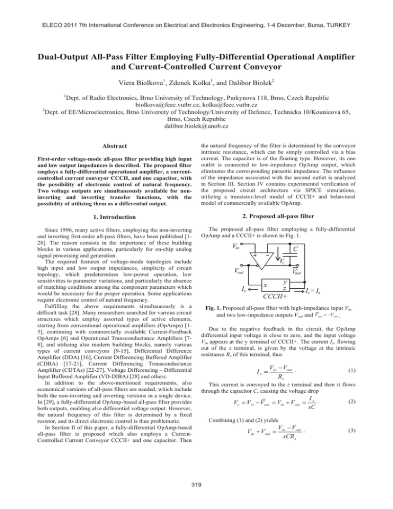
ELECO 2011 7th International Conference on Electrical and Electronics Engineering, 1-4 December, Bursa, TURKEY Dual-Output All-Pass Filter Employing Fully-Differential Operational Amplifier and Current-Controlled Current Conveyor Viera Biolkova1, Zdenek Kolka1, and Dalibor Biolek2 1 Dept. of Radio Electronics, Brno University of Technology, Purkynova 118, Brno, Czech Republic biolkova@feec.vutbr.cz, kolka@feec.vutbr.cz 2 Dept. of EE/Microelectronics, Brno University of Technology/University of Defence, Technicka 10/Kounicova 65, Brno, Czech Republic dalibor.biolek@unob.cz First-order voltage-mode all-pass filter providing high input and low output impedances is described. The proposed filter employs a fully-differential operational amplifier, a currentcontrolled current conveyor CCCII, and one capacitor, with the possibility of electronic control of natural frequency. Two voltage outputs are simultaneously available for noninverting and inverting transfer functions, with the possibility of utilizing them as a differential output. the natural frequency of the filter is determined by the conveyor intrinsic resistance, which can be simply controlled via a bias current. The capacitor is of the floating type. However, its one outlet is connected to low-impedance OpAmp output, which eliminates the corresponding parasitic impedance. The influence of the impedance associated with the second outlet is analyzed in Section III. Section IV contains experimental verification of the proposed circuit architecture via SPICE simulations, utilizing a transistor-level model of CCCII+ and behavioral model of commercially available OpAmp. 1. Introduction 2. Proposed all-pass filter Since 1996, many active filters, employing the non-inverting and inverting first-order all-pass filters, have been published [128]. The reason consists in the importance of these building blocks in various applications, particularly for on-chip analog signal processing and generation. The required features of voltage-mode topologies include high input and low output impedances, simplicity of circuit topology, which predetermines low-power operation, low sensitivities to parameter variations, and particularly the absence of matching conditions among the component parameters which would be necessary for the proper operation. Some applications require electronic control of natural frequency. Fulfilling the above requirements simultaneously is a difficult task [28]. Many researchers searched for various circuit structures which employ assorted types of active elements, starting from conventional operational amplifiers (OpAmps) [15], continuing with commercially available Current-Feedback OpAmps [6] and Operational Transconductance Amplifiers [78], and utilizing also modern building blocks, namely various types of current conveyors [9-15], Differential Difference Amplifier (DDA) [16], Current Differencing Buffered Amplifier (CDBA) [17-21], Current Differencing Transconductance Amplifier (CDTAs) [22-27], Voltage Differencing – Differential Input Buffered Amplifier (VD-DIBA) [28] and others. In addition to the above-mentioned requirements, also economical versions of all-pass filters are needed, which include both the non-inverting and inverting versions in a single device. In [29], a fully-differential OpAmp-based all-pass filter provides both outputs, enabling also differential voltage output. However, the natural frequency of this filter is determined by a fixed resistor, and its direct electronic control is thus problematic. In Section II of this paper, a fully-differential OpAmp-based all-pass filter is proposed which also employs a CurrentControlled Current Conveyor CCCII+ and one capacitor. Then The proposed all-pass filter employing a fully-differential OpAmp and a CCCII+ is shown in Fig. 1. Abstract Vin C Vc Vout Ix Vout y z CCCII+ x Iz= Ix Fig. 1. Proposed all-pass filter with high-impedance input Vin and two low-impedance outputs Vout and Vout " !Vout . Due to the negative feedback in the circuit, the OpAmp differential input voltage is close to zero, and the input voltage Vin appears at the y terminal of CCCII+. The current Ix, flowing out of the x terminal, is given by the voltage at the intrinsic resistance Rx of this terminal, thus Ix " Vin ! Vout . Rx (1) This current is conveyed to the z terminal and then it flows through the capacitor C, causing the voltage drop 319 Vc " Vin ! Vout " Vin # Vout " Ix . sC (2) Combining (1) and (2) yields Vin # Vout " Vin ! Vout . sCR x (3) ELECO 2011 7th International Conference on Electrical and Electronics Engineering, 1-4 December, Bursa, TURKEY The filter transfer function is then 1 ! sCR x . Vout V " ! out " Vin Vin 1 # sCR x VT 2I B (6) which is directly proportional to the bias current. The temperature dependence can be advantageously utilized in various temperature sensors such as temperature/phase shift converters or temperature/frequency converters (when the allpass cell is a part of sinusoidal oscillator). Vout y z Cp x Rx Iz= & Ix %Vy CCCCII+ Fig. 2. Simplified model for error analysis of filter from Fig. 1. where Rx' is the resistance Rx modified by the influence of OpAmp output resistance Ro: Rx' " Rx # Ro . LFG " % ! The theoretical small-signal behavior of the filter, described by Eq. (4), is affected by several non-idealities. Transfer function (4) can be influenced by the following real properties of the active and passive elements: OpAmp input and output impedances, parasitic impedances of conveyor terminals, ESR (Equivalent Serial Resistance) and parasitic pin impedances of the capacitor, “alpha” and “beta” factors of the current conveyor, defined by the equations Vx " % V y ! Rx I x , I z " &I x , (7) and the frequency dependence of key parameters, particularly the OpAmp gain and current conveyor “alpha” and beta” factors. The above parameters were included in the model of the filter in Fig. 1, and the approximate symbolic analysis of transfer function (4) was performed via SNAP symbolic program [31]. Numerical values of the component parameters considered are from Section IV. Dominant sources of the imperfections in the frequency responses within a given frequency range, revealed via such an analysis, are indicated in Fig. 2: “alpha” and “beta” factors of the current conveyor, and Rp and Cp parasitic elements, which model the parasitic impedances of the terminals of current conveyor, OpAmp, and capacitor C. Other parasitic impedances do not manifest themselves due to low-impedance OpAmp outputs. Taking into account the above non-idealities, filter transfer function (4) is in a more general form: C # Cp Rx' !s Rx' &R p & , CRx' 1# s (9) Note that the low-frequency gain (LFG) and the highfrequency gain (HFG) are as follows: 3. Non-ideal case Vout V " ! out " Vin Vin Vout (5) 1 2 IB " CR x VT C %! Rp Ix where VT is the thermal voltage. Thus (4) represents typical transfer functions of the non-inverting and inverting first-order all-pass filter with the natural frequency $0 " C (4) Note that Rx can be electronically adjusted via the bias current IB according to the equation [30] Rx " Vin C Rx' , HFG " 1 # p . C &R p (10) Their ratio, which is equal to one in the ideal case, can serve as a rough measure of parasitic passband ripple. Note that the high-frequency gain has a tendency to be higher than one, which can be eliminated via selecting large capacitance C >> Cp. On the other hand, the low-frequency gain has a tendency to be smaller than one, particularly for % < 1. This tendency can be reduced via selecting small intrinsic resistance Rx << Rp. Note that the above conclusions about the high-frequency gain do not take the high-frequency behavior of active elements into account. After a simple arrangement of Eq. (8) we obtain 1! s C Rx' Vout V & " ! out " # Vin Vin 1 C ' # s Rx Cp Rx' !s R'x &R p & . (11) CRx' 1# s % !1! & & The first term on the right side of (11) represents the transfer function of ideal all-pass filter with the natural frequency $0' " & CRx' "& Rx . $0 Rx' (12) The second term can be interpreted as an additional error term. At the natural frequency (12), its absolute value is 2 (8) & 320 2 ' * -C * + % ! 1 ! Rx ( # + p ( + &R p () +, C () . err " , 2 (13) ELECO 2011 7th International Conference on Electrical and Electronics Engineering, 1-4 December, Bursa, TURKEY This value (err) can serve for the estimation of a global error which is caused by the real influences. Since the “beta” factor is normally declined from its ideal value 1 by several per cent points, it can be a dominant error source in comparison to Rp and Cp, which normally differ by several decades from Rx and C. For example, when %=&=0.95, Rx' /Rp=Cp/C=10-4, then err "! 0.035, LFG "! 0.950, HFG " 1.0001. (14) The first value means that the error term in (11) is by 29 dB less than the first term, which represents the ideal all-pass filter with natural frequency (12). This error is mainly caused by the imperfection of the “beta” term, which is also responsible for the decreased low-frequency gain. The high-frequency gain is almost ideal, since it is not influenced by the “beta” factor. At the natural frequency $0 (6) of ideal non-inverting allpass filter with transfer function (4), the phase shift is exactly 90.. The impact of the real properties can be also measured by comparing this frequency with the frequency $ 0'' , at which the same phase shift appears in the non-ideal case. An analysis of Eq. (8) leads to the following result: $0'' "& $0 %! 1# Rx' &R p . Cp (15) C It should be noted that there are several reasons for decreasing the frequency of the -90. phase shift due to real influences: Decreasing the alpha and beta factors below 1, large parasitic capacitance Cp, and the Rx/Rp ratio when it cannot be neglected. The bias current IB = 50 /A corresponds to the intrinsic resistance Rx = 258.6 0 for a temperature of 27 .C (see Eq. 5). For the capacitance C = 6.16 nF, the theoretical natural frequency from (6) is 100 kHz. With regard to the low-voltage model of CCCII, the lowvoltage fully differential rail-rail OpAmp LTC6403-1 was also used in the filter, together with its SPICE model from [33]. Its supply voltages were chosen the same as for the CCCII. Table 1. Transistor models, adopted from [30]. .model PX PNP +RB=327 IRB=0 RBM=24.55 RC=50 RE=3 +IS=73.5E-18 EG=1.206 XTI=1.7 XTB=1.866 BF=110 +IKF=2.359E-3 NF=1 VAF=51.8 ISE=25.1E-16 NE=1.650 +BR=0.4745 IKR=6.478E-3 NR=1 VAR=9.96 ISC=0 NC=2 +TF=0.610E-9 TR=0.610E-8 CJE=0.180E-12 VJE=0.5 +MJE=0.28 CJC=0.164E-12 VJC=0.8 MJC=0.4 XCJC=0.037 +CJS=1.03E-12 VJS=0.55 MJS=0.35 FC=0.5 .model NX NPN +RB=524.6 IRB=0 RBM=25 RC=50 RE=1 +IS=121E-18 EG=1.206 XTI=2 XTB=1.538 BF=137.5 +IKF=6.974E-3 NF=1 VAF=159.4 ISE=36E-16 NE=1.713 +BR=0.7258 IKR=2.198E-3 NR=1 VAR=10.73 ISC=0 NC=2 +TF=0.425E-9 TR=0.425E-8 CJE=0.214E-12 VJE=0.5 +MJE=0.28 CJC=0.983E-13 VJC=0.5 MJC=0.3 XCJC=0.034 +CJS=0.913E-12 VJS=0.64 MJS=0.4 FC=0.5 In the first step, a DC analysis of the designed filter from Fig. 1 was performed with the input voltage swept within the range of -1V to +1V, see Fig. 4. For Vin = 0, the differential DC gain is approximately 11.001 for both outputs. Linear operation is guaranteed approximately for abs(Vin) < 0.63V. For larger input voltages, the nonlinearity of CCCII becomes dominant. 4. Spice simulations Vout, Vout [V] 1.0 -Vin In order to verify the feasibility of the proposed all-pass filter, a PSPICE simulation of the structure in Fig. 1 was performed. Vin Vout 0.5 0.0 -0.5 Vout -1.0 -1.0 -0.5 0.0 Vin [V] 0.5 1.0 Fig. 4. DC analysis of proposed all-pass filter from Fig. 1. Fig. 3. Transistor-level model of CCCII, adopted from [30]. The transistor-level modeling of the CCCII was performed according to [30], see Fig. 3. Since only the single-output conveyor is used in Fig. 1, transistors Q14 and Q15 are omitted in the model. As in [30], the PNP and NPN transistors were modeled with the parameters of the PR200N and NR200N bipolar transistors of ALA400 transistor array from AT&T [32], see Table I. Symmetrical supply voltages of ±1.5 V were used. The frequency responses of the filter from Fig. 1 are shown in Fig. 5, demonstrating the natural frequency control via the bias current. For IB = 50 /A, the frequency measured for -90. phase shift of the non-inverting cell is 92 kHz, which is ca 8 per cent below its theoretical value. This decrease is due to the real properties modeled by Eq. (15). The transient analysis confirmed the filter stability. For IB=500/A and sinusoidal excitation with a frequency of 1 MHz, the THD factor was 0.88% for an amplitude of 10 mV and 5.48% for 100 mV. 321 ELECO 2011 7th International Conference on Electrical and Electronics Engineering, 1-4 December, Bursa, TURKEY 6 Vout/Vin [dB] 7. References [1] 4 2 [2] 0 -2 [3] IB [uA]: 50, 100, 200, 500 -4 -6 1k 180 10k 100k frequency [Hz] 1M [4] 10M ph(Vout) [deg] [5] 135 90 Vout 45 IB [uA]: 50, 100, 200, 500 2 [6] 0 -45 -90 Vout [7] -135 -180 1k 10k 100k frequency [Hz] 1M 10M [8] Fig. 5. Simulated amplitude and phase frequency responses for various values of bias current IB. 5. Conclusions [9] The proposed first-order all-pass filter provides both noninverting and inverting outputs simultaneously. It can be also used for generating a differential voltage output with double voltage swing in comparison with the single-ended solution. Due to the utilization of fully differential operational amplifier, the filter topology exhibits high-input and low-output impedances, which enables an easy cascade synthesis. The natural frequency can be tuned electronically via modifying the intrinsic resistance of the CCCII x terminal. As a certain drawback can bee seen in that the floating capacitor with the capacitance C is employed. However, one of its outlets is connected directly to the OpAmp low-impedance output. The influence of the parasitic impedance of the second outlet is analyzed in Section III, with the conclusion that it causes a modification of the natural frequency. This modification is negligible when the parasitic capacitance is much smaller than C. If necessary, this phenomenon can be easily compensated via a modification of C. [10] [11] [12] [13] [14] [15] 6. Acknowledgment This work has been supported by the project CZ.1.07/2.3.00/20.0007 WICOMT of the operational program Education for competitiveness. [16] This work has been also supported by the Czech Science Foundation under grants Nos. 102/09/1628 and P102/10/1665, and by the research programmes of BUT No. MSM0021630503/513 and UD Brno No. MO FVT0000403, Czech Republic. [17] 322 J. E. B. Ponsonby, “Active all-pass filter using a differential operational amplifier,” Electronics Letters, vol. 2, pp. 134-135, 1966. R. Genin, “Realization of an all-pass transfer function using operational amplifiers,” Proceedings of the IEEE, vol. 56, pp. 1746-1747, 1968. P. Aronhime, and A. Budak, “An operational amplifier allpass network,” Proceedings of the IEEE, vol. 57, pp. 16771678, 1969. A. M. Soliman, “Realization of operational amplifier allpass networks,” Electronics Letters, vol. 9, pp. 67-68, 1973. T. C. Donald, J. C. David, and R. G. Jason, “A high frequency integrable band-pass filter configuration,” IEEE Transactions on Circuits and Systems – II, vol. 44, pp. 856860, 1997. S. Kilinc, and U. Cam, “Current-mode first-order allpass filter employing single current operational amplifier,” Analog Integrated Circuits and Signal Processing, vol. 41, pp. 47–53, 2004. L. Acosta, A. J.R-Angulo, A. J. L-Martín, and R. G. Carvajal, “Low-voltage first-order fully differential CMOS all-pass filter with programmable pole-zero,” Electronics Letters, vol. 45, pp. 385-386, 2009. A. Ü. Keskin, K. Pal, and E. Hancioglu, “Resistorless firstorder all-pass filter with electronic tuning,” International Journal of Electronics and Communications (AEÜ), vol. 62, pp. 304-306, 2008. A. M. Soliman, “Inductorless Realization of an All-Pass Transfer Function Using the Current Conveyor,” IEEE Transactions on Circuit Theory, vol. CT-20, pp. 80-81, 1973. A. M. Soliman, “Another Realization of an All-Pass or a Notch Filter Using a Current Conveyor,” International Journal of Electronics, vol. 35, pp. 135-136, 1973. S. Maheshwari, and I. A. Khan, “Novel first-order allpass sections using a single CCIII,” International Journal of Electronics, vol. 88, pp. 773–778, 2001. M. A. Ibrahim, H. Kuntman, and O. Cicekoglu, “Firstorder all-pass filter canonical in the number of resistors and capacitors employing a single DDCC,” Circuits Systems and Signal Processing, vol. 22, pp. 525-536, 2003. S. Maheshwari, “New voltage and current-mode APS using current controlled conveyor,” International Journal of Electronics, vol. 91, pp. 735-743, 2004. J. W. Horng, “Current conveyors based allpass filters and quadrature oscillators employing grounded capacitors and resistors,” Computers and Electrical Engineering, vol. 31, pp. 81–92, 2005. B. Metin, O. Cicekoglu, and K. Pal, “DDCC based all-pass filters using minimum number of passive elements,” Proc. of the MWSCAS 2007, pp. 518-521, 2007. A. Toker, and S. Ozoguz, “Novel all-pass filter section using differential difference amplifier,” International Journal of Electronics and Communications (AEÜ), vol. 58, pp. 153–155, 2004. A. Toker, S. Ozoguz, O. Cicekoglu, and C. Acar, “Currentmode allpass filters using current differencing buffered amplifier and a new high-Q bandpass filter configuration,” IEEE Transactions on Circuits and Systems-II: Analog and Digital Signal Processing, vol. 47, pp. 949-954, 2000. ELECO 2011 7th International Conference on Electrical and Electronics Engineering, 1-4 December, Bursa, TURKEY [18] A. Ü. Keskin, “Multi-function biquad using single CDBA,” [19] [20] [21] [22] [23] [24] [25] [26] [27] [28] [29] [30] [31] [32] [33] Electrical Engineering, vol. 88, pp. 353-356, doi: 10.1007/s00202-004-0289-4, 2006. S. Maheshwari, “Voltage-mode all-pass filters including minimum component count circuits,” Active and Passive Electronic Components, vol. 2007, Article ID 79159, 5 pages, 2007. A. Lahiri, “Comment on “Voltage-mode all-pass filters including minimum component count circuits,”. Active and Passive Electronic Components, vol. 2009, Article ID 595324, 4 pages, 2009. B. Metin, O. Cicekoglu, and K. Pal, “Voltage mode allpass filter with a single current differencing buffered amplifier,” Proc. of the MWSCAS, pp. 734-737, 2008. A. Ü. Keskin, and D. Biolek, “Current mode quadrature oscillator using current differencing transconductance amplifiers (CDTA),” IEE Proceedings: Circuits, Devices and Systems, vol. 153, pp. 214-218, 2006. N. A. Shah, M. Quadri, and S. Z. Iqbal, “CDTA based transimpedance type first-order all-pass filter,” WSEAS Transactions on Electronics, vol. 5, pp. 280-284, 2008. W. Tanjaroen, and W. Tangsrirat, “Resistorless currentmode first-order allpass filter using CDTAs,” Proc. Int. Conf. ECTI-CON, pp. 721–724, 2008. C. Tanaphatsiri, W. Jaikla, and M. Siripruchyanun, “An electronically controllable voltage-mode first-order all-pass filter using only single CCCDTA,” Proc. 2008 Int. Symposium on Communications and Information Technologies (ISCIT 2008), pp. 305-309, 2008. A. Lahiri, and A. Chowdhury, “A Novel First-Order Current-Mode All-Pass Filter Using CDTA,” Radioengineering, vol. 18, pp. 300-305, 2009. D. Biolek, and V. Biolkova, “Allpass filter employing one grounded capacitor and one active element,” Electronics Letters, vol. 45, pp. 807-808, 2009. D. Biolek, and V. Biolkova, “First-order voltage-mode allpass filter employing one active element and one grounded capacitor,” Analog Integrated Circuits and Signal Processing, vol. 65, pp. 123-129, 2010. D. Biolek, D., and V. Biolkova, “All-Pass Filters Employing Differential Op-Amps,” Electronics World, vol. 116, pp. 44-45, 2010. M. Siripruchyanun, and W. Jaikla, “Three-input singleoutput electronically controllable dual-mode universal biquad filter using DO-CCCIIs,” Active and Passive Electronic Components, vol. 2007, Article ID 36849, 6 pages, 2007. Z. Kolka, D. Biolek, and V. Biolkova, “Symbolic Analysis of Linear Circuits with Modern Active Elements,” WSEAS Transactions. on Electronics, vol. 5, pp. 88-96, 2008. D. R. Frey, “Log-domain filtering: An approach to currentmode filtering,” IEE Proceedings G: Circuits, Devices & Systems, vol. 140, pp. 406-416, 1993. LTC6403-1 – 200MHz, Low Noise, Low Power Fully Differential Input/Output Amplifier/Driver. Linear Technology, 64031fa, 2008, LT 0309 REV A, http://www.linear.com/product/LTC6403-1. 323
