www.ursi.org
advertisement
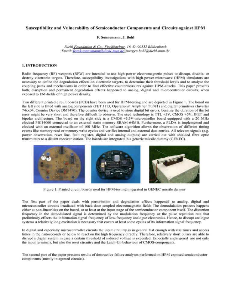
Susceptibility and Vulnerability of Semiconductor Components and Circuits against HPM F. Sonnemann, J. Bohl Diehl Foundation & Co., Fischbachstr. 16, D–90552 Röthenbach Email: frank.sonnemann@diehl-mun.de, juergen.bohl@diehl-mun.de 1. INTRODUCTION Radio-frequency (RF) weapons (RFW) are intended to use high-power electromagnetic pulses to disrupt, disable, or destroy electronic targets. Therefore, susceptibility investigations with high-power-microwave (HPM) simulators are necessary to define the degradation effects on electronic targets, to determine their threshold levels and to analyse the coupling paths and mechanisms in order to find effective countermeasures against HPM-attacks. This paper presents both, disruption and permanent degradation effects happened to analog, digital and microcontroller circuits, when exposed to EM-fields of high power density. Two different printed circuit boards (PCB) have been used for HPM-testing and are depicted in Figure 1. The board on the left side is fitted with analog components (FET J113, Operational Amplifier TL081) and digital primitives (Inverter 74xx04, Counter Device DM7490). The counter device is used to store digital bit errors, because the duration of the bit error might be very short and therefore difficult to observe. The used technology is TTL +5V, CMOS +5V, JFET and bipolar architecture. The board on the right side is a CMOS +3.3V-microntroller board equipped with a 20 MHz clocked PIC14000 connected to an external static memory SRAM 64MB. Furthermore, a PLDA is implemented and clocked with an external oscillator of 100 MHz. The software algorithm allows the observation of different timing events like memory read or memory write cycles and verifies internal and external data entries. All relevant signals (e.g. power observation, reset line, fault register, digital and analog outputs) are carried out with shielded fibre optic transmitters to a distant receiver station. The boards are integrated in a generic missile dummy (GENEC). Figure 1: Printed circuit boards used for HPM-testing integrated in GENEC missile dummy The first part of the paper deals with perturbation and degradation effects happened to analog, digital and microcontroller circuits irradiated with back-door coupled electromagnetic fields The demodulation process happens either at non-linearities on the board, or at least at the input stage of the semiconductor component itself. The distortion frequency in the demodulated signal is determined by the modulation frequency or the pulse repetition rate that preliminary effects the information signal frequency of low-frequency analogue electronics. Hence, to disrupt analogue systems a relatively long excitation is necessary that covers at least some cycles of its information signal frequency. In digital and especially microcontroller circuits the input circuitry is in general fast enough with rise times and access times in the nanoseconds or below to react on the high frequency directly. Therefore, relatively short pulses are able to disrupt a digital system in case a certain threshold of induced voltage is exceeded. Especially endangered are not only the input terminals, but also the reset circuitry and the Latch-Up behaviour of CMOS-components. The second part of the paper presents results of destructive failure analyses performed on HPM exposed semiconductor components (mostly integrated circuits). 2. NON DESTRUCTIVE EFFECTS The observed threshold field strength when interference occur depend on the pulse frequency, the angle of incidence (AoI) and the polarisation. These parameters define the resonances of the structural dimensions and the capability of the RF-field to penetrate from the outer to the inner including the coupling to the wiring and the wiring resonances. The RF-voltage generated at the input of the semiconductor degrades analog signals and changes digital states. The analog degradation in the GENEC is observed to be connected with the RF-LF-conversion at nonlinearities of the semiconductor which forms the RF-signal envelope in a demodulation process. The demodulated signal then is able to travel along the LF-circuit path like an intended signal. In a low pass analog electronic circuit as well as in automatic gain control circuits the interference amplitude is observed to increase with the pulse repetition rate, in a band pass analog electronic circuit the interference amplitude is highest if the repetition rate is equal to the center frequency of the pass band. Very high pulse repetition rates (much higher than the information signal frequency) lead often to a suppression of the information signal, either by generating a significant offset shift (Figure 2), or by driving a PIcontroller into its saturation (e.g. AGC circuits). 6.550 10 Hz 6.425 6.300 6.550 100 Hz 6.425 6.300 200 Hz 6.550 6.425 6.300 320 Hz 6.550 6.425 6.300 0.00 1.25 2.50 3.75 5.00 Figure 2: Distortion of the time signal of a low pass analog system for different pulse repetition rates In the digital LSI-74 circuits the induced voltage peaks are able to change the digital states in clocked and non clocked systems. Above a defined field strength each field pulse produces a state change. In MSI clocked circuits the probability for one HPM pulse to change the state increases with the field amplitude. On the microcontroller board the first faults happened are HPM-induced resets, that can be distinguished in two kind of faults: the so called master-clear-reset (MCLR) that is similar to the reset button on a standard PC and the power-on-reset (POR), that is activated when the power supply voltage drops below a certain level. Then, the microcontroller is in an idle state for a defined time (for the used PIC it is 75 ms) to guarantee that the power recovers during that time (Figure 3). With an increase of the applying fieldstrength, the access to the memory is denied or the memory looses its volatile data. A malfunction of the internal PIC microcontroller program can also happen, even when it is unpowered. VDD LWL3 R=10k Chip_Reset~ MCLR~ C=100n VDD PIC 14000 PIC_E PIC_Sz VDD rise detect HPM_T LWL4 HPM 6 3 0 6 3 0 6 3 0 T0904_20.tsp 75ms 75ms [s] 0 50 100 150 200 250 300 350 400 450 500 Figure 3: Reset-circuitry and HPM induced power-on reset (POR) For UWB and HPM non destructive latch up effects occurred in the MSI-GENEC circuits. A single field pulse forced the semiconductor to a self-holding short-circuit between 3.3V power and ground. In most cases the circuit withstood the regulator limited current. However the 3.3V supply dropped down and forced the additional connected circuits into a quasi unpowered state. Higher field strength produced destructive semiconductor defects which are discussed below. 3. DESTRUCTIVE EFFECTS The HPM induced conditions are considered harmful only when the operating conditions of the component are violated by • Input voltages exceeding the dielectric breakdown strength of the intrinsic oxide or inter-metal isolation and causing punch-through or flashover • Input / output voltages putting junctions into reverse biased breakdown and causing low resistive current bypasses or high local power dissipation • Supply voltages reverse biasing the component and causing high current surges The primary degradation mechanisms can be grouped into two distinctly different classes: • dielectric breakdown: the induced voltage strains an insulating material beyond its dielectric breakdown resistance and an electron avalanche effect initiates local punch-through or flashover. The short discharge current transports metal atoms along the path of discharge leaving a permanently conductive channel. • junction breakdown: The induced voltage strains a junction into reverse bias exceeding the breakdown voltage, the strength of the electrical field in the depletion zone initiates the generation of secondary electron / hole pairs. A permanent damage is only possible, when the junction temperature exceeds the maximum operating conditions. The avalanche effect supports a reverse current flow, hot charge carriers may trigger parasitic thyristors (LatchUp). The dielectric breakdown fieldstrength is in the order of 5*105 V/cm for the silicon-oxide or nitride components used in semiconductor manufacturing. Assuming a channel width between 1 µm to 10 µm, the corresponding dielectric breakdown voltage yields 50 – 500 V. The junction breakdown voltages are significantly lower in the order of 10 – 40 V (e.g. breakdown voltage emitter / base with feature size of 0.2 – 0.3 µm is approx. 6 to 10 V). Therefore, it is assumed that the dielectric breakdown happens much faster before the junction starts to be conductive and before the transient propagates to the protective components. To estimate a value for the required rise-time the dielectric surface breakdown (flashover) is compared to the behaviour of surface discharge switches. These can be operated in the self-breakdown mode by overvolting them with fast–rising voltage pulses. Rise times in the order of dv/dt > 1kV/ns are reported (H.M. von Bergmann, Surface Discharge Switches, Gas Discharge closing switches, A. Guenther, M. Kristiansen, Plenum Press, 1990). The dielectric breakdown along the surface of an insulator is referred to as flash-over. The left picture in Figure 4 shows a flashover between bond pad and ground metallization ring of the DM7404 inverter (TTL) with historically established design-rules (> 5 µm). The low degree of damage indicates that no significant amount of energy was discharged into the area of the flash-over after the HPM-pulse ceased. The right picture in Figure 4 shows the degraded area of the input protection diode close to the affected bond pad of a PIC microcontroller after HPM pulse irradiation. The visible damage of degraded metallization is certainly not generated by induced HPM energy alone, but supported by other energy either transformed through demodulation and intermediate storage and/or by energy stored at the component (e.g. decoupling capacitors). The bond pad metallization shows reflowed and discoloured areas with one spot of evaporated metal, the metallization of the diode several ares of reflow and discoloration. As the duration of the associated degeneration process does not correlate to the duration of the HPM pulse this type of damage is clearly allocated to secondary damage. Figure 4: Flashover DM7404 and Input Protection Diode Destruction of the PIC14000 4. CONCLUSION The influences of HPM and UWB on electronic systems are two-fold: the coupled (HF) interference and voltages on the wiring caused by HF-LF conversion effects in nonlinearities can cause LF interference within the electronic wiring superimposed on the useful signals and negatively influencing the system performance. At a higher fieldstrength HPM and UWB can induce such high voltages within the electronic circuit that components are physically destroyed. Although network analysing programmes in general allow signal levels exceeding the limits of semiconductors, in reality new effects appear which are not considered in the modelling of the simulation programs. In no way can destruction mechanisms be rebuilt with the available network tools. Real measurements have to be done for this. A component analysis of destroyed components is used to determine a connection between the HPM radiation characteristics, the coupling path and the amount of destruction. REFERENCES [1] J.Bohl, T.Ehlen, F.Sonnemann „HPM-Effects in LF-Electronic-Circuits: A Numerical Approach“, EUROEM98, Tel-Aviv, Israel, June 1998. [2] T.Ehlen, J.Bohl, F.Sonnemann „Electromagnetic Coupling Paths to Electronic Systems Connected withElectronic Setups and Destruction Mechanism“, IST/SET Symposium 98, Aalborg, Denmark, October 1998. [3] D. Taylor, D.V. Giri, “High-Power Microwave Systems and Effects ”, Taylor&Francis, 1994 [4] J. Benford, Swegle, “High-Power Microwaves ”, Artech House, 1992 [5] R. E. Richardson,“Modeling of Low-Level Rectification RFI in Bipolar Circuitry“, IEEE Trans Electromagnetic Compatibility, vol. EMC-21.No. 4, Nov. 1979. [6] J. Bohl, T.Ehlen, G. Staines, F. Sonnemann, „ Interference and Destruktion Mechanisms of Electronic Irradiated with HPM and UWB Sources“ , ICEAA01, September 2001, Turin, Italy
