VR Enable and Discharge SLG7NT4100
advertisement
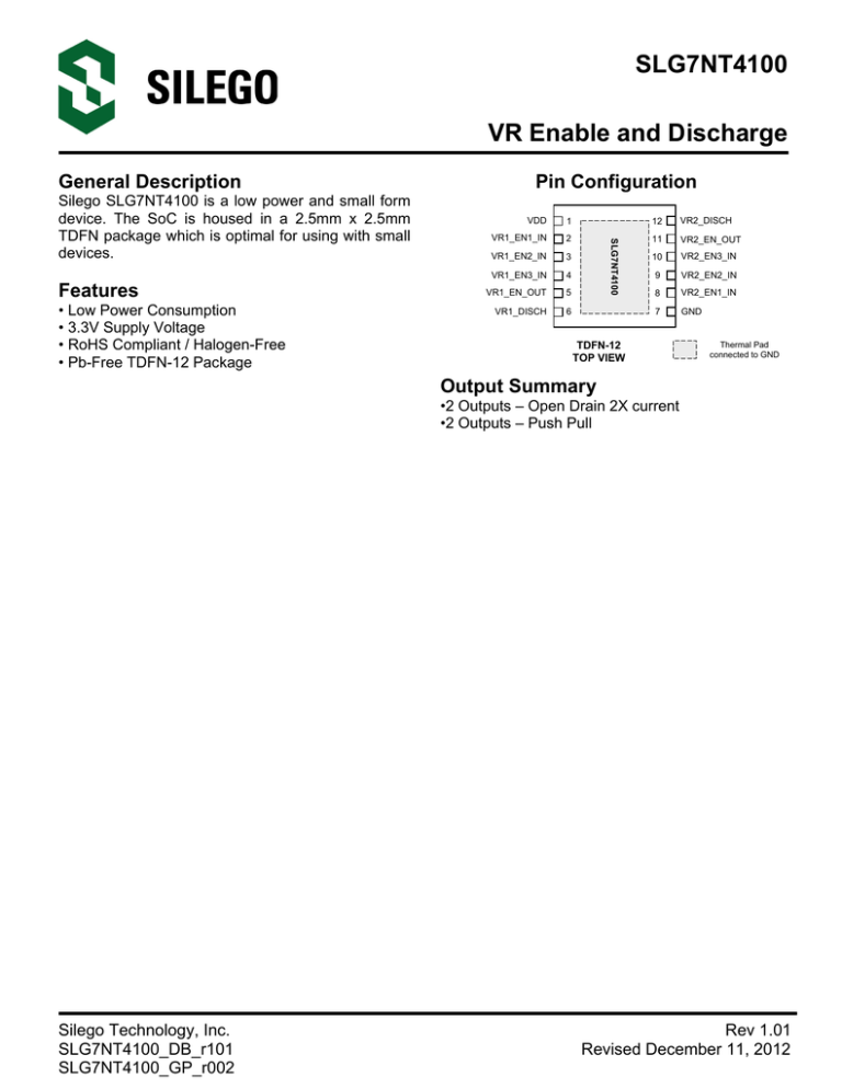
SLG7NT4100 VR Enable and Discharge General Description Features • Low Power Consumption • 3.3V Supply Voltage • RoHS Compliant / Halogen-Free • Pb-Free TDFN-12 Package Pin Configuration VDD 1 12 VR2_DISCH VR1_EN1_IN 2 11 VR2_EN_OUT VR1_EN2_IN 3 10 VR2_EN3_IN VR1_EN3_IN 4 VR1_EN_OUT 5 VR1_DISCH 6 SLG7NT4100 Silego SLG7NT4100 is a low power and small form device. The SoC is housed in a 2.5mm x 2.5mm TDFN package which is optimal for using with small devices. 9 VR2_EN2_IN 8 VR2_EN1_IN 7 GND TDFN-12 TOP VIEW Thermal Pad connected to GND Output Summary •2 Outputs – Open Drain 2X current •2 Outputs – Push Pull Silego Technology, Inc. SLG7NT4100_DB_r101 SLG7NT4100_GP_r002 Rev 1.01 Revised December 11, 2012 SLG7NT4100 VR Enable and Discharge Block Diagram Typical Application Circuit +3.3V C1 100nF IN IN IN VR1_EN1_IN VR1_EN2_IN VR1_EN3_IN 1 2 3 4 5 6 U1 VDD data I/O data I data I/O data I/O data I/O data I/O data I/O data I/O data I/O data I/O GND 12 11 10 9 8 7 VR2_DISCH VR2_EN_OUT OUT OUT SLG7NT4100 VR1_DISCH IN IN IN SLG7NT4100_DB_r101 VR2_EN1_IN VR1_EN_OUT VR2_EN2_IN OUT OUT VR2_EN3_IN Page 2 SLG7NT4100 VR Enable and Discharge Pin Configuration Pin # 1 2 3 4 5 6 7 8 9 10 11 12 Exposed Bottom Pad Pin Name VDD VR1_EN1_IN VR1_EN2_IN VR1_EN3_IN VR1_EN_OUT VR1_DISCH GND VR2_EN1_IN VR2_EN2_IN VR2_EN3_IN VR2_EN_OUT VR2_DISCH Exposed Bottom Pad Type Power Input Input Input Output Output GND Input Input Input Output Output GND Pin Description Supply Voltage Digital Input Digital Input Digital Input Push Pull Open Drain 2x current Ground Digital Input Digital Input Digital Input Push Pull Open Drain 2x current Ground Ordering Information Part Number SLG7NT4100V SLG7NT4100VTR SLG7NT4100_DB_r101 Package Type V = TDFN-12 VTR = TDFN-12 - Tape and Reel (3k units) Page 3 SLG7NT4100 VR Enable and Discharge Absolute Maximum Conditions Parameter Min. Max. Unit VHIGH to GND -0.3 7 V Voltage at input pins -0.3 7 V Current at input pin -1.0 1.0 mA Storage temperature range -65 150 °C Junction temperature -- 150 °C Electrical Characteristics (@ 25°C, unless otherwise stated) Symbol VDD Parameter Condition/Note Supply Voltage Typ. Max. Unit 3.0 3.3 3.6 V -- 1 -- μA -40 25 85 °C -100 -- 100 nA IQ Quiescent Current TA Operating Temperature IL Input Leakage Current Leakage Current for Digital Inputs or outputs in High impedance state VIH HIGH-Level Input Voltage Logic Input at VDD=3.3V 1.8 -- -- V VIL LOW-Level Input Voltage Logic Input at VDD=3.3V -- -- 1.1 V VOH Output Voltage High Push Pull Logic Level Output at VDD=3.3V, IOH=3mA 2.1 -- -- V VOL Output Voltage Low Push Pull Logic Level Output at VDD=3.3V, IOL=3mA -- -- 0.81 V VOL Output Voltage Low Open Drain Logic Level Output at VDD=3.3V, IOL=10mA, 2X Drive -- -- 0.252 V VO Maximal Voltage Applied to any PIN in High-Impedance State -- -- VDD V IOL LOW-Level Output Current Push Pull Current at, VOL=0.4V -- 1 -- mA IOL LOW-Level Output Current Open Drain Current at VOL=0.4V, 2X Drive 28 -- -- mA TSU Start up Time After VDD reaches 1.6V -- 7 -- ms SLG7NT4100_DB_r101 Static inputs and outputs Min. Page 4 SLG7NT4100 VR Enable and Discharge Timing Diagrams SLG7NT4100_DB_r101 Page 5 SLG7NT4100 VR Enable and Discharge Package Top Marking Datasheet Revision 1.01 SLG7NT4100_DB_r101 Programming Code Number 02 Part Code Revision Date 4100V AB 12/11/2012 Page 6 SLG7NT4100 VR Enable and Discharge Package Drawing and Dimensions 12 Lead TDFN Package JEDEC MO-229, Variation WDDE SLG7NT4100_DB_r101 Page 7 SLG7NT4100 VR Enable and Discharge Tape and Reel Specification # of Package Type Pins TDFN 12L 2.5x2.5mm 0.4P Green 12 Max Units Nominal Package Size (mm) per reel 2.5x2.5x0.75 3000 Trailer A per box Reel & Hub Size (mm) Pockets 3000 178/60 42 Leader B Pocket (mm) Length Length Pockets (mm) (mm) 168 42 168 Width Pitch 8 4 Carrier Tape Drawing and Dimensions Package Type TDFN 12L 2.5x2.5mm 0.4P Green Pocket BTM Length (mm) Pocket BTM Width (mm) Pocket Depth (mm) Index Hole Pitch (mm) Pocket Pitch (mm) Index Hole Diameter (mm) A0 B0 K0 P0 P1 D0 E F W 2.75 2.75 1.05 4 4 1.55 1.75 3.5 8 Index Hole Index Hole to Tape to Pocket Tape Width Edge Center (mm) (mm) (mm) Recommended Reflow Soldering Profile Please see IPC/JEDEC J-STD-020: latest revision for reflow profile based on package volume of 4.6875 mm3 (nominal). More information can be found at www.jedec.org. SLG7NT4100_DB_r101 Page 8 SLG7NT4100 VR Enable and Discharge Silego Website & Support Silego Technology Website Silego Technology provides online support via our website at http://www.silego.com/.This website is used as a means to make files and information easily available to customers. For more information regarding Silego Green products, please visit: http://greenpak.silego.com/ http://greenpak2.silego.com/ http://greenfet.silego.com/ http://greenfet2.silego.com/ http://greenclk.silego.com/ Products are also available for purchase directly from Silego at the Silego Online Store at http://store.silego.com/. Silego Technical Support Datasheets and errata, application notes and example designs, user guides, and hardware support documents and the latest software releases are available at the Silego website or can be requested directly at info@silego.com. For specific GreenPAK design or applications questions and support please send email requests to GreenPAK@silego.com Users of Silego products can receive assistance through several channels: Online Live Support Silego Technology has live video technical assistance and sales support available at http://www.silego.com/. Please ask our live web receptionist to schedule a 1 on 1 training session with one of our application engineers. Contact Your Local Sales Representative Customers can contact their local sales representative or field application engineer (FAE) for support. Local sales offices are also available to help customers. More information regarding your local representative is available at the Silego website or send a request to info@silego.com Contact Silego Directly Silego can be contacted directly via e-mail at info@silego.com or user submission form, located at the following URL: http://support.silego.com/ Other Information The latest Silego Technology press releases, listing of seminars and events, listings of world wide Silego Technology offices and representatives are all available at http://www.silego.com/ THIS PRODUCT HAS BEEN DESIGNED AND QUALIFIED FOR THE CONSUMER MARKET. APPLICATIONS OR USES AS CRITICAL COMPONENTS IN LIFE SUPPORT DEVICES OR SYSTEMS ARE NOT AUTHORIZED. SILEGO TECHNOLOGY DOES NOT ASSUME ANY LIABILITY ARISING OUT OF SUCH APPLICATIONS OR USES OF ITS PRODUCTS. SILEGO TECHNOLOGY RESERVES THE RIGHT TO IMPROVE PRODUCT DESIGN, FUNCTIONS AND RELIABILITY WITHOUT NOTICE. SLG7NT4100_DB_r101 Page 9
